
Design of a 50M Transimpedance Amplifier with 0.98fa/Hz Input
Inferred Noise in a 0.18M CMOS Technology
William Wilson and Tom Chen
Department of Electrical and Computer Engineering, Colorado State University, Fort Collins, U.S.A.
Keywords: Biosensor, Electrochemical Detection, Electrochemistry Frontend, Low Noise, Low Power,
Transimpedance Amplifier (TIA), Switched Capacitor Integrator.
Abstract: Low noise and low power consumption are key requirements for high performance electrochemical
biosensors. Noise performance directly affects the sensor’s ability to detect small amounts of target
chemical compounds. These requirements present challenges for the design of frontend circuitry in
electrochemical biosensors. These challenges are especially apparent for integrated electrochemical
biosensor arrays, as sensor size is limited by tissue cell size and the desire to achieve a cellular scale
resolution. This paper presents a low-noise and low-power transimpedance amplifier (TIA) intended for (but
not limited to) use as an analog frontend in an electrochemical biosensor. The amplifier was designed on a
commercial 0.18µm CMOS process. The overall design achieves a 50M transimpedance gain with
981aA/Hz input inferred noise, 8.06µW power consumption at 0.9V power supply, and occupies an overall
silicon area of 0.0074mm
2
. To our best knowledge, the design presented in this paper achieved the best
noise performance and power consumption among transimpedance amplifier designs reported to date.
1 INTRODUCTION
Biosensor devices have found an increasingly broad
range of applications, including but not limited to
clinical testing, biological research, environmental
testing, and pharmaceutical testing. With ever
increasing applications for biosensors, the
requirements of detection hardware in biosensors are
covering an increasingly broad range of bio-signals.
These signals often require very specifically
designed detection hardware, for example, to
account for very weak input signal coupled with
high input noise.
Additionally, the ability to visualize the
molecules of cellular communication allows us to
further understand the biology that drives normal
and pathophysiological processes. Electrochemical
sensor arrays provide new opportunities for
chemical vision without the addition of labels, such
as chromophores or fluorophores. The growing
interest in high density electrochemical sensor arrays
(Xu et al., 2002; Qi et al., 2003) dictates a size
requirement for the sensor’s electronics which often
conflicts with achieving low noise and low power
consumption per read channel. This paper presents
the design of an electrochemical sensor frontend for
an integrated sensor array design. Given the
stringent constraints on physical size of sensor
electronics and low input signal level due to small
electrode sizes, the goal of the design is to achieve
low input inferred noise and low power
consumption. These goals must be met while also
maintaining the speed requirement of a 1 KHz input
signal bandwidth and small electronic footprint.
2 BIOSENSING TECHNIQUES
Sensing techniques currently in use include
fluorescence spectroscopy, bioluminescence and
chemilluminescence detection, and electrochemical
detection. Fluorescence spectroscopy is a process of
adding and tracking fluorescent light-responsive
dyes or “label” molecules in a sample. Bio and
chemilluminescence detection rely on the detection
of a naturally luminescent substance in an analyte.
Electrochemical detection uses a reduction or
oxidation reaction (i.e. a redox process) to detect an
electrochemically active analyte.
112
Wilson W. and Chen T..
Design of a 50MO Transimpedance Amplifier with 0.98fa/vHz Input Inferred Noise in a 0.18µM CMOS Technology.
DOI: 10.5220/0004786801120119
In Proceedings of the International Conference on Biomedical Electronics and Devices (BIODEVICES-2014), pages 112-119
ISBN: 978-989-758-013-0
Copyright
c
2014 SCITEPRESS (Science and Technology Publications, Lda.)

2.1 Fluorescence Detection
Fluorescence imaging detection involves adding a
fluorescent label to the sample material. As shown in
Figure 1, a filtered light source is used to create a
single frequency excitation light. Application of the
excitation light causes a photon emission at different
frequency, allowing detection of the fluorescent
label.
Figure 1: Fluorescence Detection Example.
Typical fluorescence detection systems use
either a high-performance single pixel detector with
a scanning excitation source, or a two-dimensional
array of detectors, such as a CCD sensor, with a
homogeneous excitation light source. In a
fluorescence detection system, possible array size is
determined by CCD implementation and the number
of photosensitive pixels (Agah, et al., 2005). In
optical based systems; however, lenses and strategic
illumination patterns can be utilized to achieve
single-molecule measurement resolutions without
the need to greatly reduce the scale of the detection
devices (Rosenstein et al., 2011).
2.2 Bio/chemilluminescence
Bioluminescence and chemilluminescence
techniques rely on the emission of light from the
analyte. Although generally (but not necessarily) in
the visible light spectrum, the small amount of light
emitted is usually not visible to the human eye.
Detection has been typically achieved with an
extremely sensitive CCD sensor and photomultiplier
tubes. CMOS image sensors have not been utilized
in bioluminescence until more recently due to poor
but improving performance and lower SNR (Agah,
et al., 2005)
2.3 Electrochemical Detection
Using a redox process, electrochemical detection can
be used in a wide range of measurements under the
condition that the analyte being measured is
electrochemically active (Wightman et al., 2006,
Villagrasa et al., 2013). Typical measurement
instrumentation includes a two or three electrode
system, where a potentiostat is used to hold a
specific potential across a sample. Setting a specific
potential between the reference (RE) and the
working electrode (WE) can be used to selectively
detect a specific analyte. The potentiostat also
sources or sinks the required current through the
counter electrode (CE). A typical three electrode
potentiostat system is shown in Figure 2.
Figure 2: Typical Three Electrode Potentiostat.
The popularity of electrochemical sensing stems
from its ability to detect a wide range of molecules.
These molecules include glucose (Liao et al., 2012),
Dopamine (Pihel et al., 1996), Nitric Oxide (Starkey,
et al., 2001), and
-Aminobutyric Acid (Niwa et al.,
1998). The electrical nature of this detection method
also makes electrochemical detection a more
suitable option for integrated sensors and sensor
arrays. The sensor circuit presented in this paper is
intended for use in high density electrochemical
sensor arrays, which provide cellular scale
resolution.
3 MOTIVATIONS FOR
INTEGRATED BIOSENSORS
Currently, typical biosensor implementations include
a custom made sensing device, ranging from single
pixel light detection sensors or single (working)
electrode electrochemical systems, all the way to
two dimensional light sensors such as CCD or
CMOS light detection sensors and multi-
dimensional electrode arrays. Many biosensor
systems must be further supported with a system of
electronics and/or software to supply the end user
with meaningful data and a useable interface. In
many implementations, designing or even setting up
the supporting electronic hardware can become more
involved or time consuming than the detection
device itself.
With discrete devices, external detection
hardware is often used, due to the readily available
forms of computer video recording devices for
Designofa50MOTransimpedanceAmplifierwith0.98fa/vHzInputInferredNoiseina0.18µMCMOSTechnology
113

CCD/CMOS video-based sensors, and the wide
range of computer interfaced potentiostat systems.
These readily available interfaces have some
limitations, including their size, lack of portability,
lack of spatial resolution, and need of trained
personnel with appropriate laboratory facilities.
3.1 Ease of Use
Many integrated solutions include supporting
hardware, such as a transimpedance amplifier (TIA)
for both photodiode based light detectors and
electrochemical detectors. Including the sensor and
detection hardware on a single chip or package with
either a wired or wireless interface simplifies the use
of the biosensor in research, and allows for greater
complexity in hardware. With an integrated system,
a user could easily connect an array of thousands of
electrodes to a computer for data acquisition using a
single connector or wireless interface, eliminating
the need for highly trained personnel and bulky
hardware. Complete sensor backend integration also
provides an abstraction of the sensor’s functionality.
This can eliminate time consuming setup and the
possibility of incorrectly connected devices.
3.2 Increased Resolution and
Applications
The use of small molecules to send signals between
cells is a hallmark of biological communication.
Understanding cellular communication allows for
greater insight regarding the biology that drives
normal and pathophysiological processes. One of the
major difficulties in understanding the actions of
small molecules is our inability to directly visualize
their release and diffusion through biological tissues.
Therefore, understanding cellular communication
through cellular level visualization is an important
goal in biomedical research. Cellular sizes of interest
typically lie within the range of a 20-50µm radius. It
is highly desirable to place electrodes with spacing
below 50µm (Henze, 2000; Hassibi, 2007). This puts
a physical limit on underlying electronics in
integrated sensor designs.
4 DESIGN CONSTRAINTS AND
REQUIREMENTS FOR
SENSOR INTEGRATION
Integrated sensors place much more stringent
physical constraints and performance requirements
on the supporting electronics. With many biological
experiments necessitating extremely small and
sensitive measurements, a high signal-to-noise ratio
(SNR) is often a high priority design requirement for
biosensor frontend circuitry.
4.1 Size and Power Constraints
Visualizing cellular communication with electrode
arrays requires the electrode pitch to be within in the
cellular scale. With parallel read channels, the
underlining electronics will have very restricted size
requirements to match electrode spacing at the
cellular scale. In addition, parallel read channels put
a greater burden on overall power consumption per
read channel for two reasons:
1. For implantable biosensors, the desirable power
consumption for the analog frontend is in the
range of a few µWatts to maximize battery life.
Low power consumption may also enable
alternative power sources such as wireless
power.
2. Perhaps more importantly, in experiments with
living tissues, the tissue must be kept at specific
temperature, humidity, and pH levels. If the
supporting circuitry dissipates an excess of
power as heat, it can be more difficult to keep
tissue samples alive and in the proper
conditions.
The necessity of lower power consumption and
small physical size often comes at the cost of noise
(Toumazou, C., et al., 2002) and accuracy (Kinget,
2005). Therefore, design of integrated biosensors
often requires careful tradeoffs and novel circuits,
especially with respect to input inferred noise.
4.2 Noise Requirement
Depending on the application and specifics of the
sensor design, the analyte detection process will
have an inherent noise level. If the input inferred
noise level of the supporting circuitry can be pushed
below the noise level of the sensor itself, the
circuitry won’t impose a limitation on the resolution
of the measurements.
In electrochemical detection systems, noise
standard deviation has been shown to vary based on
electrode area. The noise standard deviation (
I
) on
indium tin oxide electrodes has been shown to
increase with the square-root of electrode area for
small electrodes, and linearly with area for larger
electrodes (Yao et al., 2012). Figure 3 shows noise
generated at the electrode-solution interface as a
function of electrode area for electrochemical
BIODEVICES2014-InternationalConferenceonBiomedicalElectronicsandDevices
114
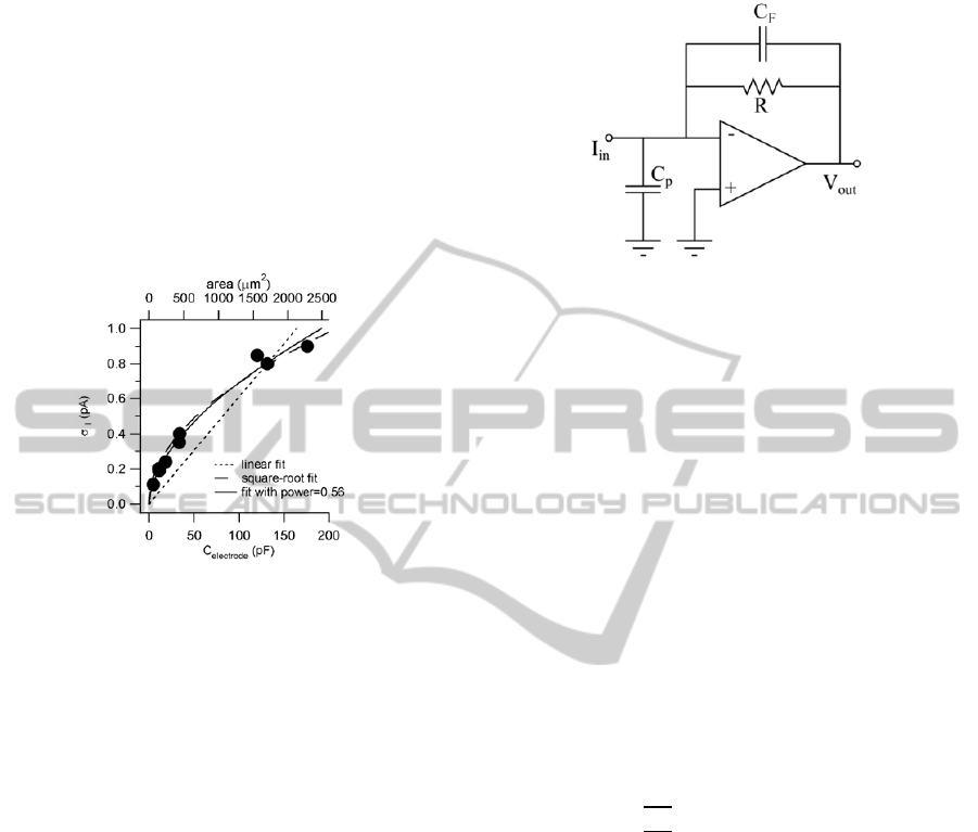
sensors. For electrodes used in highly integrated
sensors, their sizes typically range from a few m
2
to tens of m
2
(Pettine et al., 2012). The standard
deviation of the inherent noise from an electrode-
solution interface can be lower than 100fA. This
puts a limit on the amount of noise that analog
biosensor frontend circuitry can generate without
compromising sensitivity. The TIA design in this
paper focuses on achieving low input inferred noise
and low power consumption while meeting other
design requirements for electrochemical sensor
arrays.
Figure 3: Noise Standard Deviation vs. Electrode Area.
5 EXISTING TIA DESIGNS
TIAs have a wide range of applications from optical
communications to Micro-Electro-Mechanical
Systems (MEMS), to sensors. Therefore, design
requirements for TIAs cover a broad range from
GHz speed for optical communication systems, to
sub-MHz speed with low power for biosensors.
Different design requirements often result in
different circuit topologies and design trade-offs.
5.1 Conventional TIA Design
A typical transimpedance amplifier design consists
of an operational amplifier with a resistive feedback
path as shown in Figure 4. A compensation
capacitor, C
F
, is often added in parallel with the
resistor in the feedback path, to help improve
instability caused by the zero created by the resistor
(R) and the parasitic input capacitance (C
P
) from the
sensor electrode.
Assuming an infinitely high op-amp gain, the
DC Transimpedance gain can be calculated simply
as
V
ou
t
= -I
in
R (1)
While the design itself is simple, several
practical issues arise in implementation. The resistor
Figure 4: Simple Resistive Feedback TIA.
size, R, is a direct function of transimpedance gain.
With high transimpedance gain, the size of the
resistor quickly approaches the limits of on-die
components. Furthermore, the absolute accuracy of
on-die resistor values is not well controlled in
modern CMOS process.
In the resistor-based topology, the zero created
by the input capacitance and feedback resistor may
need to be cancelled with a feedback capacitor for
overall stability. In a biosensor system, the parasitic
capacitance level can vary from one electrode to the
next, and change depending on the medium in which
the electrodes are placed, making this a difficult
design problem in large electrode arrays.
Noise performance of the resistor-based design
may not be suitable for biosensing applications.
Assuming a linear resistance, the noise current in a
50M resistor at room temperature can be
calculated as
i
n
=
= 33.23fA/Hz
(2)
This noise floor doesn’t consider the additional
noise generated in the OTA, but rather the just the
noise in the feedback network itself. This noise floor
is considered higher than the acceptable level,
depending on the inherent noise level determined by
the electrode area and chemical reaction.
5.2 Novel Continuous Time TIA
Designs
One method of avoiding the large resistor needed for
high gain and high sensitive TIA design is the use of
a resistor T-network to generate a large effective
feedback resistance with smaller physical resistors.
This topology can be used to achieve both a high
transimpedance gain and low noise. (Sharma et al.,
2007). Although this topology requires significantly
less total resistance on chip than its equivalent
Designofa50MOTransimpedanceAmplifierwith0.98fa/vHzInputInferredNoiseina0.18µMCMOSTechnology
115
single-resistor counterpart, the overall size reduction
is often still not at the level required by designs of
highly integrated biosensor arrays.
An alternative TIA implementation employs the
use of an active current reducing circuit in place of
the resistor (Ferrari, et al., 2009). This type of design
can be used to emulate very high equivalent
resistances of hundreds of G with relatively high
linearity. This design implements the current
reducing circuit using a series of operational
amplifiers which can increase power consumption
while still maintaining a reasonable die area. This
increased level of power consumption may not be
suitable due to the stringent operating temperature
requirements of live tissue on our biosensor
applications. This design does manage to achieve an
extremely low input noise level.
Two other continuous time implementations
involve using an active load and ratio of capacitors
to generate high effective transimpedance gains
(Razavi, 2000; Salvia, 2009). These designs tend to
rely on extremely high impedance input biasing
circuits, which can consume large amounts of die
area. Despite this fact, this topology does tend to
produce respectable input noise specifications.
5.3 Switched-Capacitor TIA Designs
Since large resistors (several to tens of M’s) can
consume large amounts of die area and can be
inaccurate once fabricated, an alternative is to
replace the resistor with a “switched capacitor.” This
can be useful in larger scale voltage amplifiers, as
well as transimpedance amplifiers. Switched
capacitor implementations are also referred to as
charge integrating transimpedance amplifiers.
Special considerations such as charge injection and
switch noise minimization or cancellation must be
taken into account when using switching circuits
with high sensitivity current measurements.
Although switching can have undesirable effects
in high sensitivity transimpedance amplifiers, it can
be used to the designer’s advantage, providing a
means to effectively cancel undesired 1/f noise and
amplifier offset through correlated double sampling.
One such design uses a slow integrator,
integrating the input current onto a capacitor and
sampling the output voltage periodically (Tang et al.,
2012). Integrator designs eliminate the need for a
large capacitor, and allow for low noise
performance. This type of design has achieved spot
noise specifications as low as 25fA/Hz.
A reduced noise floor is one of the main
advantages of low-speed switched integrator
designs. Allowing the signal to integrate over an
extended period of time produces a reduction in
switching noise and charge injection, leading to the
potential for a lower overall input inferred noise
current.
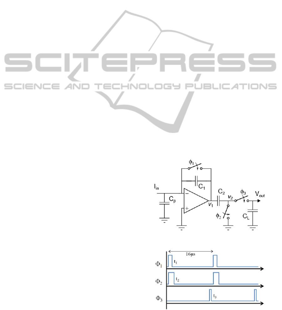
6 PROPOSED TIA DESIGN
The proposed TIA design consists of a switched
capacitor transimpedance amplifier (SCTIA) design
with a dedicated three-phase clock scheme to
perform correlated double sampling. An optimized
Class-C inverter based operational amplifier is used
in a slow integrating switched capacitor topology.
The TIA topology is shown in Figure 5. Although
this circuit topology has been proposed before by
Tang et al. (Tang et al., 2012), our design uses an
optimized Class-C inverter based operational
transconductance amplifier (OTA) to further reduce
the input inferred noise. The optimized OTA
achieves improved noise performance as we
illustrate it in this section.
Clock phase timing is shown in Figure 6, and
example input response is shown in Figure 7. Basic
circuit operation is as follows: during
1
, the
charges on C
1
and C
2
are set to 0. During the time
that
1
is low, C
1
is charged with the input current.
The voltage V
1
changes with a slope proportional to
the magnitude of the input current. V
2
follows the
change in V
1
after
2
goes low.
Figure 5: Top level SCTIA schematic.
Figure 6: Clock Phase Timing.
BIODEVICES2014-InternationalConferenceonBiomedicalElectronicsandDevices
116
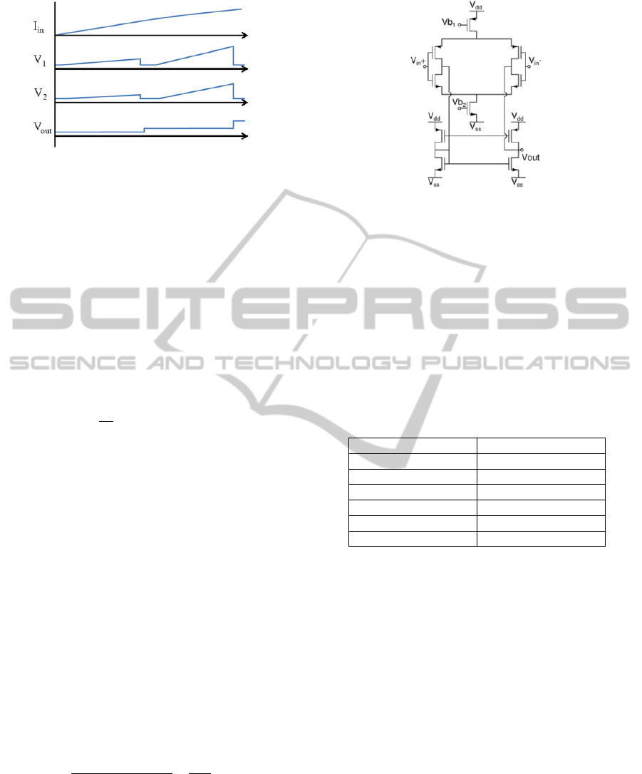
Figure 7: Example Input Response.
During
2
, the OTA offset as well as 1/f noise is
stored as a voltage V
err
on C
2
. At the end of
2
, the
opamp output is subtracted by v
err
, effectively
removing the low frequency noise and offset. At this
point, the voltage V
2
consists only the desired signal.
The switch controlled by
3
along with the circuit
load (next amplification stage, or output
capacitance) serves as a sample and hold, which
holds the output voltage until the end of the next
period. With t
2
and t
3
indicated in Figure 6, the TIA
output voltage at the end of each clock period can be
expressed as
1
(3)
The Class-C inverter-based OTA topology is
shown in Figure 8 (Wilson, et al., 2013). To reduce
power consumption, the OTA is operated at 0.9V
supply voltage as opposed to the nominal 1.8V
supply voltage for the 0.18m CMOS process. Table
1 summarizes OTA performance. The enhanced
transconductance of the inverter-based OTA
topology allows greater stability and lower power
consumption without compromising its DC gain and
bandwidth.
The inverter-based topology uses both p and n-
type input transistors, effectively achieving double
the transconductance of a single input transistor
(Figueiredo et al., 2010). Assuming the p and n
transistors are balanced, and the equivalent noise
resistances for the n and p type transistors are R
Nn
,
and R
Np
, respectively, the equivalent noise resistance
for the inverter based amplifier is
2
(4)
Since the noise of the TIA is a function of both
OTA noise and feedback network noise (Wilson, et
al.), this lowered equivalent noise resistance leads to
a decreased overall noise.
Figure 8: Inverter-Based OTA Topology.
When designing the OTA, the load and input
inverters should be sized in such a way that
and
are balanced, and the output is biased at half the
supply voltage when the input is set to half the
supply voltage. The input transistors should be large
enough to sufficiently reduce voltage offset, and all
transistor pairs should be matched in layout. The tail
transistors should be used to control the current
through the input transistors and provide common
mode rejection.
Table 1: OTA Performance Specifications.
DC Gain 58.6dB
-3dB Bandwidth 22kHz
Unity Gain Freq. 10.2MHz
Power 8.06µW@0.9V
Phase Margin 53.06°
PSRR 50.4dB
Layout Area 75µm x 51.5µm
7 SIMULATION RESULTS AND
PERFORMANCE
COMPARISON
The proposed TIA circuit was implemented using a
commercial 0.18µm CMOS process. Figure 9 shows
the layout of the overall circuit, measuring 93.5µm
by 78.5µm. Figure 10 shows simulation of
sinusoidal current input on the layout extracted
netlist. The input current has a peak value of 1nA
with 1 kHz frequency. This signal magnitude and
frequency are derived by the maximum requirement
for amperometry signals from a number of chemical
compounds, including dopamine, norepinephrine,
and nitric oxide. The overall peak-to-peak output
voltage is approximately 100mV, showing a
transimpedance gain of 50M. A low power
consumption of 8.06µW is achieved by operating the
Designofa50MOTransimpedanceAmplifierwith0.98fa/vHzInputInferredNoiseina0.18µMCMOSTechnology
117
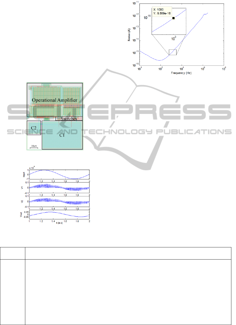
OTA deep in subthreshold. The power consumption
of the circuit is also greatly reduced by the use of a
low power supply voltage. The input inferred noise
(shown in Figure 11) was found using a periodic
steady state (PSS) analysis.
The circuit is run with a 62.5 kHz clock,
allowing ample time for input current integration.
Due to the high transimpedance gain and low power
supply, the circuit output voltage can begin to
saturate, causing a high level of distortion with a
current input of about 5nA.
The measured performance for the designs
discussed in this paper is included in Table 2.
Figure 9: Overall Layout of SCTIA Design.
Figure 10: Extracted Layout Simulation Results.
Figure 11: Input Inferred Noise vs. Frequency.
8 CONCLUSIONS
In this paper a low power switched capacitor
integrating transimpedance amplifier design was
presented. This design uses an optimized Class-C
inverter-based amplifier in a switched capacitor
topology to achieve a low noise floor. The
cancellation of errors due to 1/f noise and amplifier
offset through the use of correlated double sampling
also contributed to the overall low input inferred
noise. To our best knowledge, this design has the
best noise and power performance among TIAs
reported in literature so far.
ACKNOWLEDGEMENTS
The authors would like to thank NSF for their
financial support (DGE0841259). Generous
technical support and silicon fabrication by
Texas
Instruments is also greatly appreciated.
Table 2: CMOS Transimpedance Amplifier Performance Comparison.
Work Razavi Salvia Ferrari Tang Sharma Zand Balasubramanian
This Work
(Simulation)
Power
30mW@3
V
436µW@
1.8V
45mW@3
V
3.2mW 400µW 30mW@3V
90µW@
1.8V
8.06µW@
0.9V
Gain
8.7k 56M 60M 88M
up to
25M
33k 150K - 550K
50M
Spot Noise
n/a
65fA/
Hz
4fA/
Hz
25fA/
Hz
88fA/
Hz @
1.6M
n/a n/a
981aA/
Hz @ 1kHz
Avg. Noise
4.5pA/H
z
n/a n/a n/a n/a
6.8pA/
Hz
1.6pA/Hz
1.08pA/Hz
Area
n/a n/a n/a n/a n/a
300µm x
155µm
n/a
93.5µm x 78.5µm
Process
0.6µm 0.18µm 0.35µm 0.35µm 0.6µm 0.35µm 0.18µm
0.18µm
BIODEVICES2014-InternationalConferenceonBiomedicalElectronicsandDevices
118

REFERENCES
Agah, A., Hassibi, A., Plummer, J., Griffin, P., 2005.
Design requirements for integrated biosensor arrays.
In Proc. SPIE 5699, Imaging, Manipulation, and
Analysis of Biomolecules and Cells: Fundamentals
and Applications III.
Balasubramanian, V., Ruedi, P.-F., Temiz, Y., Ferretti,
A., Guiducci, C., Enz, C.C., 2013. A 0.18
mbiosensor front-end based on 1/f noise, distortion
cancelation and chopper stabilization techniques. In
Biomedical Circuits and Systems, IEEE
Transactions on, vol.PP, no.99, pp.1,14.
Ferrari, G., Gozzini, F., Molari, A., Sampietro, M., 2009.
Transimpedance Amplifier for High Sensitivity
Current Measurements on Nanodevices. In Solid-
State Circuits, IEEE Journal of, vol.44, no.5,
pp.1609,1616.
Figueiredo, M., Santin, E., Goes,J., Santos-Tavares, R.,
Evans, G., 2010. Two-stage fully-differential
inverter-based self-biased CMOS amplifier with
high efficiency. In Circuits and Systems (ISCAS),
Proceedings of 2010 IEEE International Symposium
on , vol., no., pp.2828-2831, May 30 2010-June 2
2010.
Hassibi, A., Vikalo, H., Hajimiri, A., 2007. On Noise
Processes and Limits of Performance in Biosensors.
In Journal of Applied Physics, vol. 102, issue 1,
2007.
Henze, D. A., Borhegyi, Z., Csicvari, J., Mamiya, A.,
Harris, K. D., Buzsáki, G., 2000. Intracellular
Features Predicted by Extracellular Recordings in
the Hippocampus in Vivo. In Journal of
Neurophysiology, Jul. 2000, pp. 390-400.
Kinget, Peter R., 2005. Device Mismatch and Tradeoffs
in the Design of Analog Circuits. In IEEE JSSC,
Vol. 40, No. 6, June 2005.
Liao, Y., et al., 2012. A 3-µW CMOS Glucose Sensor
for Wireless Contact-Lens Tear Glucose Monitoring.
In IEEE JSSC, Vol. 47, No. 1, Jan. 2012.
Niwa, O., et al. 1998. Small-Volume On-Line Sensor for
Continuous Measurement of -Aminobutyric Acid.
In Analytical Chemistry, 1998, 70, 89-93.
Pettine, W., Jibson, M., Chen, T. Tobet, S., Henry, C.,
2012. Charaterization of novel microelectrode
geometries for detection of neurotransmitters. In
IEEE Sensors Journal, Vol.12, No. 5, May, 2012.
Pihel, K., et al., 1996. Overoxidized Polypyrrole-Coated
Carbon Fiber Microelectrodes for Dopamine
Measurements with Fast-Scan Cyclic Voltammetry.
In Anal. Chem. 1996, 68, pp. 2084-2089.
Qi, P., et al., 2003. Toward Large Arrays of Multiplex
Functionalized Carbon Nanotube Sensors for Highly
Sensitive and Selective Molecular Detection. In
Nano Lett, 2003, No. 2. 2003.
Razavi, B., 2000. A 622 Mb/s 4.5 pA//spl radic/Hz
CMOS transimpedance amplifier [for optical
receiver front-end]. In Solid-State Circuits
Conference, 2000. Digest of Technical Papers.
ISSCC. 2000 IEEE International , vol., no.,
pp.162,163, 9-9 Feb. 2000.
Rosenstein, J., Sorgenfrei, S., Shepard, K.L., 2011.
Noise and bandwidth performance of single-
molecule biosensors. In Custom Integrated Circuits
Confer
ence (CICC), 2011 IEEE , vol., no., pp.1,7,
19-21 Sept. 2011.
Salvia, J., Lajevardi, P., Hekmat, M., Murmann, B.,
2009. A 56M CMOS TIA for MEMS applications.
In Custom Integrated Circuits Conference, 2009.
CICC '09. IEEE , vol., no., pp.199,202, 13-16 Sept.
2009.
Sharma, A., Zaman, M.F., Ayazi, F., 2007. A 104-dB
Dynamic Range Transimpedance-Based CMOS
ASIC for Tuning Fork Microgyroscopes. In Solid-
State Circuits, IEEE Journal of , vol.42, no.8,
pp.1790,1802, Aug. 2007.
Starkey, S., et al., 2001. A rapid and transient synthesis
of nitric oxide (NO) by a constitutively expressed
type II NO synthase in the guinea-pig
suprachiasmatic nucleus. In British Journal of
Pharmacology (2001) 134, 1084-1092.
Tang,Y., Zhang, Y., Fedder, G.K., Carley, L.R., 2012.
An ultra-low noise Switched Capacitor
Transimpedance Amplifier for parallel Scanning
Tunneling Microscopy. In Sensors, 2012 IEEE , vol.,
no., pp.1,4, 28-31 Oct. 2012.
Toumazou, C., et al., 2002 Tradeoffs in Analog Circuit
Design. Springer, 2002.
Villagrasa, J.P., Colomer-Farrarons, J., Miribel P.L.,
2013. Bioelectronics for Amperometric Biosensors,
State of the Art in Biosensors - General Aspects, Dr.
Toonika Rinken (Ed.), ISBN: 978-953-51-1004-0,
InTech.
Wilson, W., Chen, T., Selby, R., 2013. A current-starved
inverter-based differential amplifier design for ultra-
low power applications. In Circuits and Systems
(LASCAS), 2013 IEEE Fourth Latin American
Symposium on, vol., no., pp.1,4, Feb. 27-March 1,
2013.
Wightman, R Mark, 2006. Probing Cellular Chemistry
in Biological Systems with Microelectrodes. In
Science, 17 March 2006, Vol. 311.
Xu, C., Lemon, W., and Lui, C., 2002. Design and
Fabrication of a High Density Metal Microelectrode
Array for Neural Recording. In Sensors and
Actuators, Vol. A 96, Issue. 1. pp. 78-85, Jan. 2002.
Yao, J., Gillis, K., 2012. Quantification of Noise Sources
for Amperometric Measurement of Quantal
Exocytosis Using Microelectrodes. In Analyst, vol.
137, issue 11, pp.2674-2681. ROYAL SOCIETY OF
CHEMISTRY.
Zand, B., Phang, K., Johns, D.A., 2001. A
transimpedance amplifier with DC-coupled
differential photodiode current sensing for wireless
optical communications. In Custom Integrated
Circuits, 2001, IEEE Conference on. , vol., no.,
pp.455,458, 2001.
Designofa50MOTransimpedanceAmplifierwith0.98fa/vHzInputInferredNoiseina0.18µMCMOSTechnology
119
