
BAlGaN-based Vertical Cavity Surface Emitting Laser Operating in
Deep UV Region
X. Li
1,2
, S. Sundaram
2
, P. Disseix
3
, S. Bouchoule
4
, G. Le Gac
3
, G. Patriarche
4
, F. Réveret
3
,
J. Leymarie
3
, Y. El Gmili
2
, J. Streque
2
, F. Genty
5
, J-P. Salvestrini
2,6
, P. L. Voss
1,2
,
R. D. Dupuis
7
and A. Ougazzaden
1,2
1
School of Electrical and Computer Engineering, Georgia Institute of Technology, GT-Lorraine, 57070 Metz, France
2
UMI 2958, Georgia Tech - CNRS, 57070 Metz, France
3
Institut Pascal UMR 6602 CNRS, Université Blaise Pascal, 63171 Aubière, France
4
LPN CNRS, UPR20, 91460 Marcoussis, France
5
Supelec, LMOPS, EA4423, 57070 Metz, France
6
Université de Lorraine, LMOPS, EA 4423, 57070 Metz, France
7
Center for Compound Semiconductors and School of Electrical and Computer Engineering,
Georgia Institute of Technology, Atlanta, Georgia 30332, U.S.A.
1 RESEARCH PROBLEM
There is a strong demand for semiconductor light
sources emitting in the DUV region for a wide
variety of potential applications such as sterilization,
water/air purification, optical imaging systems,
spectroscopy, or high density storage systems.
However, the primary limitation of current
applications is the existing UV sources. The
conventional UV light sources are excimer lasers,
mercury lamps or Nd: YAG lasers. These sources
suffer from low level of performance, low reliability,
significant size, and the toxic substances. Compared
with conventional lasers, the semiconductor light-
emitting devices are an ideal choice due to their
reliability, compactness and high efficiency.
Besides, the wavelength could be tuned by changing
the compositions of the active region. UV
semiconductor light sources are of great
technological interest in our daily lives.
Among semiconductor laser devices, VCSEL is
one of the most attractive configurations: The
emission light from VCSEL is perpendicular to the
surface, so it could be integrated into two
dimensional arrays. 10000 devices could be
integrated on one wafer to give high output. Circular
beam makes it easy for coupling into the fiber. It
consists of high reflectivity distributed Bragg
reflector (DBR) mirrors, which enables low
threshold and high output. Besides, it could be tested
during processing which decreases the
manufacturing cost. Compared with EELs, it has low
temperature sensitivity due to its single longitudinal
cavity.
AlGaInN-based wide bandgap semiconductor
material systems have brought innovative changes in
photonic devices, which allow the operating
wavelengths of LEDs and lasers to reach a spectral
range spanning from blue to DUV. However, the III-
nitride VCSELs demonstrated so far operate in the
wavelengths of visible violet and blue spectral
range, while no efficient VCSELs emitting below
300 nm were reported. To extend the VCSEL
emission to the ultraviolet region, the challenges lie
in many aspects. Firstly, there is a degradation of the
structural quality of heteroepitaxial AlGaN materials
with increasing Al molar ratio and lack of high
quality AlN substrates. High dislocation density for
the structure grown on foreign substrates would lead
to low internal quantum efficiency (IQE). Secondly,
AlGaN MQWs suffer from the strong quantum-
confined Stark effect (QCSE) induced by
piezoelectric and spontaneous polarization, which
leads to the separation of electrons and holes and
reduces significantly the emission efficiency. C-
plane AlGaN alloys also exhibit anisotropic optical
polarization properties: E-field c polarized
emission (which will be referred to as TE
polarization) decreases when compared to the
emission polarized along the c axis (E-field // c) as
the Al composition increases for the deep UV
wavelengths, which is harmful to surface-emission.
Thirdly, high-reflectivity distributive Bragg reflector
26
LI X., Sundaram S., Disseix P., Bouchoule S., Le Gac G., Patriarche G., Réveret F., Leymarie J., Gmili Y., Streque J., Genty F., Salvestrini J., Voss P.,
Dupuis R. and Ougazzaden A..
BAlGaN-based Vertical Cavity Surface Emitting Laser Operating in Deep UV Region.
Copyright
c
2015 SCITEPRESS (Science and Technology Publications, Lda.)

(DBR) with large bandwidth for the DUV VCSELs
is a big challenge, considering the limited refractive
index contrast and large lattice mismatch for
conventionally used AlGaN/Al(Ga)N structures.
Based on the challenges mentioned above, in the
framework of developing DUV VCSELs for this
work, TE-emission enhanced AlGaN MQWs
emitting at 280 nm grown on relaxed AlGaN buffer,
new BAlN material system which can have big
refractive index contrast with Al(Ga)N and its
applications to DBRs would be studied and
explored.
2 OUTLINE OF OBJECTIVES
The objective of this thesis is to develop efficient
vertical cavity surface-emitting lasers operating
below 300 nm. The final structure consists of
dielectric top mirror, AlGaN active region and
bottom DBR based on BAlGaN material system.
The first part of the work is addressed to the
AlGaN active region, including the study of AlGaN
epitaxial growth for the control of composition and
strain relaxation, the realization of TE-enhanced
MQWs design and the related characterizations. The
purpose is to develop efficient DUV MQWs with
improved TE emission.
The second part focuses on the growth of novel
BAlN material, in order to study the influence of
growth conditions and characteristics of the material.
The third part would be the design and
realization of DBRs, including both BAlGaN DBRs
and conventional AlGaN DBRs as reference.
The final goal is to realize DUV devices: laser
diodes, RC-LEDs and ultimate VCSELs.
3 STATE OF THE ART
Visible and UV-VCSELs and edge-emitting lasers
(EELs) based upon the wide bandgap
semiconductors including ZnSe- and GaN-based
material systems have been extensively explored for
the potential applications of high density optical
storage system, laser printer engines, full color
display systems, and large-area projector systems.
The ZnSe-based materials were the first material
system to provide continuous wave operation of
blue-green EELs (Ding et al. 1990). However,
serious reliability problems possibly arising from its
chemically and structurally unstable material system,
have hindered the application of ZnSe lasers in the
real-world systems. Later, AlGaInN-based wide
bandgap semiconductor material systems (Gil 1998;
McIntosh et al. 1996) have brought innovative
changes in photonic devices, which enable the
operating wavelengths of LEDs and lasers to reach a
spectral range from blue to UV (Shatalov et al.
2002). The first nitride-based injection laser centered
at around 390 nm was demonstrated in 1995
(Akasaki et al. 1995). AlGaN-based UV LEDs for
wavelength shorter than 360 nm was initiated in
1998 (Han et al. 1998). Then UV and DUV light
devices have undergo tremendous evolution through
rapid progress in material growth, device fabrication
and packaging. In the DUV range, the LEDs and
EELs have progressed a lot. The group of Sensor
Electric Technology has reported high external
quantum efficiency of 10.4% at 20 mA continuous
current with output power up to 9.3 mW for
encapsulated AlGaN LEDs emitting at 278 nm
(Shatalov et al. 2012). UV Craftory has developed
commercial production of 50 mW AlGaN LEDs
with wavelength ranging from 255 nm to 355 nm
which have 10% external quantum efficiency (EQE)
and over 10000 hours life time (Ippommatsu et al.
2013). For AlGaN lasers, the group of Technische
Universität Berlin has reported laser grown on AlN
bulk emitting at 279 nm with threshold of 50 mJ/cm
2
(IQE 20~30%), and laser grown on ELO (epitaxially
laterally overgrown) AlN/sapphire template emitting
at 272 nm with threshold of 65 mJ/cm
2
(IQE
10~20%). Both of two are TE-polarization dominant
(Martens et al. 2014). (Xie et al. 2013) reported low
threshold power of 84 kW/cm
2
for lasing at 280.8
nm and (Johnson et al. 2012) demonstrated lasing at
266 nm with threshold of 41 kW/cm
2
. Both of
devices are based on the AlGaN MQWs grown on
single crystal AlN bulk substrates. To achieve IQE
higher than 60%, AlN bulk single crystal can be
used since its threading dislocation density is below
510
8
cm
-2
(Hirayama et al. 2014), but it suffers
from high impurity absorption, high cost and limited
availability. Riken group has used ammonia pulsed-
flow multilayer growth to fabricate AlN template on
sapphire to obtain IQE of 60% from AlGaN QWs
(Hirayama et al. 2007; Hirayama et al. 2014).
Recently, for the devices grown on AlN templates
on sapphire, simulated emission was observed at
wavelengths of 256 nm and 249 nm with thresholds
of 61 kW/cm
2
and 95 kW/cm
2
at room temperature,
as reported by (X.-H. Li et al. 2014).
The development of III-nitride-based VCSELs
includes optically-pumped devices at blue
wavelengths (Redwing et al. 1996; Krestnikov &
Ledentsov 1999), and room temperature CW lasing
BAlGaN-basedVerticalCavitySurfaceEmittingLaserOperatinginDeepUVRegion
27

VCSELs by current injection for blue/violet
wavelengths (Higuchi et al. 2008; Lin et al. 2014;
Kasahara et al. 2011). So far, no efficient VCSELs
operating below 300 nm were reported.
One of the biggest challenges for UV VCSELs
lies in the need for high reflectivity DBRs.
Conventional AlInGaN based DBRs have been
explored to give high reflectivity from blue to the
near-UV region. For example, 25-pair
Al
0.18
Ga
0.82
N/Al
0.8
Ga
0.2
N has a reflectivity as high as
99% with bandwidth of 26 nm at central wavelength
of 347 nm (Mitrofanov et al. 2006). Below 300 nm,
(Moe et al. 2006) have demonstrated reflectivity of
66% and 83% for the shortest wavelengths of 245
nm and 279 nm, using 10 and 21 pairs of
AlGaN/AlN, respectively. It is difficult to achieve
high reflectivity requirement due to large absorption
and small refractive index contrast of the materials
in DUV region. Conventionally used AlGaN layers
exhibit large lattice mismatch as high as ~2.4%
between GaN and AlN to achieve only small
refractive index contrast in the mirror structure. The
high reflectivity requiring large number of pairs was
accompanied by the dislocations, cracks or rough
interfaces. So the novel system is necessary to build
efficient DBR structures below 300 nm.
In this thesis, BAlGaN material system would be
used to achieve the target. The primary reason for
the B incorporation is that a very small amount of B
in AlN could introduce a strong refractive index
contrast (Watanabe et al. 2003; Abid et al. 2012).
For example, BAlN with only 1.2% B can have a
refractive index contrast of 0.17 with AlN. Besides,
BAlN system exhibits less optical absorption than
AlGaN due to its large bandgap. Additionally, both
the large refractive index contrast and strain-
compensated structure could be obtained at the same
time by alternating BAlN and AlGaN layers in the
DBR.
4 METHODOLOGY
The growth was performed in a MOVPE T-shape
reactor (Gautier et al. 2007) under 100 Torr.
Hydrogen was used as carrier gas. Trimethyl-
aluminum (TMAl), thrimethyl-gallium (TMGa),
triethylborane (TEB) and NH
3
were used as
precursors for aluminum, gallium, boron and
nitrogen, respectively. 900-nm thick AlN templates
on c-axis sapphire and 3 μm GaN templates on c-
axis sapphire were used as substrates.
High resolution X-ray diffraction (XRD)
measurements were performed in a Panalytical
X’pert Pro MRD system with Cu Κα radiation to
determine composition and other structural
information. The depth concentration profiles for
different elements were performed by secondary ion
mass spectroscopy (SIMS) analysis.
Surface morphology was characterized by atomic
force microscope (AFM) and scanning electron
microscope (SEM). The sample was then prepared
for scanning transmission microscopy (STEM) using
focused ion beam (FIB) thinning and ionmilling. 100
nm carbon was deposited before FIB in order to
protect the surface. High-angle annular dark field
scanning transmission microscopy (HAADF-STEM)
characterizations were performed on aberration-
corrected JEOL 2200FS electron transmission
microscope.
The optical properties were investigated by
photoluminescence (PL) and depth-resolved
cathodoluminescence (CL) techniques. The PL
excitation at 266 nm was provided by the second
harmonic generation of a continuous laser. The
emission is analyzed by a 1 m focal length
monochronometer and detected by a CCD camera.
Both the optical excitation and light collection are
from sample surface. Optical transmission
measurements were performed under Xenon arc
lamp excitation for determination of the absorption
band-edge and absorption coefficients in the wells.
5 EXPECTED OUTCOME
This work is in the framework of developing DUV
VCSELs based on new BAlGaN material system.
The main research work includes AlGaN active
region, bottom DBR based on new BAlGaN material
and final laser devices. The expected outcome of this
thesis contains following part:
MOVPE growth study for AlGaN layers
including a careful control of composition and
strain state.
Design and growth of AlGaN MQWs structure
which preserves the oscillator strength of TE-
polarized transition.
MOVPE growth study for new BAlN material
including its growth conditions and structural
characteristics.
Achievement of DUV DBRs based on
BAlN/Al(Ga)N system.
Realization of AlGaN-based DUV lasers, and
BAlGaN-based RCLEDs and VCSELs.
PHOTOPTICS2015-DoctoralConsortium
28
6 STAGE OF THE RESEARCH
The whole work can be divided into three sections:
AlGaN active region, BAlGaN DBRs and final
devices. Obtained results are presented in subsection
6.1 and 6.2, while the next plans are listed in
subsection 6.3.
6.1 DUV AlGaN MQWs
The first part was concentrated in the optimization
of AlGaN layers and AlGaN MQWs emitting at 280
nm.
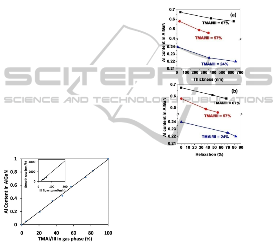
6.1.1 AlGaN Composition and Relaxation
In order to obtain a good control over composition
and relaxation for AlGaN growth, a series of AlGaN
single layers were grown on AlN templates. The
relationship between composition and TMAl/III
ratio as wells as thickness and relaxation has been
established. For the fully-strained thin layers below
critical thickness, Al composition in the solid phase
varies linearly with the TMAl relative concentration
shown in Fig. 1. Additionally, the AlGaN growth
rate, shown in the inset, varies linearly with the total
III elements flow (TMAl+TMGa) while the V/III
ratio remains constant, which indicates that the
growth occurs in a mass transport limited regime.
Figure 1: Al composition of AlGaN layers fully-strained
on AlN templates Vs. TMAl/(TMAl+TMGa) ratio. The
inset shows the growth rate versus total flow rate of
(TMAl+TMGa).
However, when the thickness of the single AlGaN
layer was increased under the same TMAl/III ratio
so that the layer relaxed, it was observed that the
average Al content in the layer decreased. This
composition fluctuation during AlGaN relaxation
has generally been ascribed to the composition
pulling effect. G.B. Stringfellow et al. explained that
the excess lattice mismatch energy would perturb the
solid composition towards the composition which
minimizes mismatch (G.B.Stringfellow 1993). The
smaller adatoms will be incorporated preferentially
at steps having relative compressive strain, and
larger adatoms under relatively tensile strain
(Tersoff 1996; Venezuela et al. 1999).
Figure 2: Al content in the AlGaN single layers plotted as
a function of (a) layer thickness, and (b) corresponding
layer relaxation for three different TMAl/(TMAl+TMGa)
ratios.
Very few studies have considered AlGaN layers
grown on AlN template which would be under
compressive strain. In the present investigation, as
shown in Fig. 2, a decrease in the Al composition of
AlGaN layers is evidenced when the layer thickness
(and hence the layer relaxation) is increased. For
three different TMAl/III ratios in the gas phase, a
clear Al content drop can be observed, confirming
the composition pulling effect. In our case, AlGaN is
under compressive strain on AlN, so in the initial
stage when the layer is fully strained, AlGaN has a
tendency towards higher Al content in order to
minimize mismatch, while for the relaxed layer case,
we see a lower Al content. Since Ga-N has a smaller
bond energy than Al-N, Ga incorporation would be
more controlled by the strain state than Al
incorporation (Reuters et al. 2012; Bogusławski et al.
2000), which means that Ga atoms are expelled out
for the initial stage under high compressive strain,
BAlGaN-basedVerticalCavitySurfaceEmittingLaserOperatinginDeepUVRegion
29
and Ga incorporation increases when the layer is
relaxed with lateral lattice increasing.
6.1.2 TE-enhanced AlGaN MQWs Design
C-plane AlGaN alloys exhibit anisotropic optical
polarization properties: E-field c polarized
emission (TE polarization) decreases when
compared to the emission polarized along the c axis
(E-field // c) as the Al composition increases for the
deep UV wavelength, which is detrimental to
surface-emission. This is attributed to the
arrangement of the valence bands at the Γ point of
Brillouin zone and Γ
7
symmetry becomes the upper
valence band for an aluminum composition typically
higher than 10% (Ryu et al. 2013; Kolbe et al. 2010;
Nam et al. 2004; Leroux et al. 2004; Leroux et al.
2002). However, it is possible to restore the
amplitude of the oscillator strength by imposing
some strain in the AlGaN QW, which can affect the
valence band states and the selection rules (Chuang
& Chang 1996; Northrup et al. 2012; Ivanov et al.
2014; Murotani et al. 2011). The strain is due to the
lattice mismatch between barriers and wells which
have different Al content. Thus, the barrier
composition can be chosen to provide sufficient
compressive strain in the wells in order to enhance
the TE-polarized optical transition.
To achieve emission at a wavelength of around
280 nm, the Al composition of the well was chosen
to be x
Al
= 0.37 and the well thickness was fixed to
1.7 nm in the calculations. The thickness of barriers
was fixed to 10 nm. Envelop function simulations
taking into account strain and built-in electric fields
have been performed for AlGaN/AlGaN MQWs
structure. The optimal Al content in barriers is
designed to be 0.57 (0.01), for which the strain (-
0.5%) introduced in the wells is sufficient to
preserve the oscillator strength of TE-polarized
optical transition and therefore surface emission.
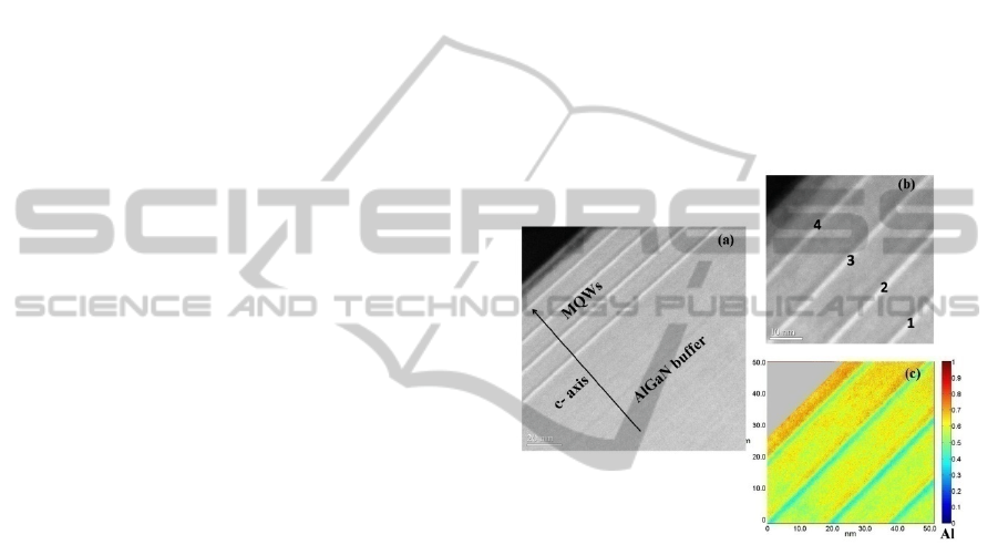
6.1.3 Growth and Characterizations of
MQWs
In order to release the strain in the barriers, a relaxed
Al
0.58
Ga
0.42
N buffer was grown on AlN template as a
pseudo-substrate. Then, 4-period Al
0.57
Ga
0.43
N /
Al
0.38
Ga
0.62
N MQWs were grown on top based on
the design. HAADF-STEM cross-section images of
MQWs and upper part of the relaxed buffer were
shown in Fig. 3(a) and 3(b). The barriers thickness is
measured to be 10 ~ 11 nm from intensity profiles
and the wells thickness is of 1.6 ~ 1.8 nm. The
average composition of barriers could be determined
from EDX quantitative analysis and was found to be
0.57 ( 0.015). Since the spatial resolution of the
EDX analysis is typically of 2 nm, in order to
determine the composition of ultra-thin wells, high-
resolution Z-contrast HAADF-STEM image was
transformed into quantitative composition mapping
by following a procedure proposed in (Pantzas et al.
2012). The background intensity has been subtracted
and thickness variation has been corrected. The
complete analysis results in a chemical mapping
were shown in Fig. 3(c). The average Al content in
the barriers is accord with EDX value (x
Al
~0.57)
and the average Al content in the wells is estimated
to be x
Al
~0.38 ( 0.015). The thickness and
composition values obtained from Figs. 3(a)-3(c) fit
well the XRD experimental data.
Figure 3: (a) Cross-section High-angle Annular Dark Field
Scanning Transmission Electron Microscopy (HAADF-
STEM) images taken along the <1 1 -2 0> zone axis for
MQWs and buffer layer; (b) High magnification of
HAADF-STEM images; (c) Al composition map obtained
from (b).
Cathodoluminescence (CL) spectra at 77 K under
different excitation energy have been shown in Fig.
4(a). Under a low excitation power of 3 keV
corresponding to a penetration depth of the electron
beam of typically 30 nm, a single emission peak
from wells at 286 nm indicates that the carriers are
mostly confined in the wells. When the excitation
power is increased to 10 keV and the penetration
depth of the excitation beam reaches 230 nm, a
luminescence signal at 262 nm appears in addition to
the emission of the wells, which is attributed to the
barriers and buffer layer. The emission at 262 nm
indeed corresponds to a bandgap energy of 4.73 eV,
which is in agreement with the experimental
composition of the barriers and buffer layer (x
Al
~
0.57). At room temperature the increase of the
PHOTOPTICS2015-DoctoralConsortium
30
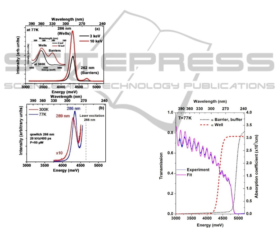
barrier luminescence with respect to 77K is
attributed to the thermal activation of carriers in the
AlGaN layers (barriers or buffer layers). In the case
of an optical in-well pumping (excitation at 266 nm)
as displayed in Fig. 4(b), the laser beam is mainly
absorbed in the QWs and not in the barriers. Thus,
only the luminescence of the wells is observed.
However, it is found that both classical
photoluminescence and cathodoluminescence
provide the same QW emission line. The linewidth
is 9.5 nm for PL at 77 K and 11.9 nm for PL at 300
K.
Figure 4: (a) Cathodoluminescence (CL) spectra at 77 K
(and at 300 K in the inset) for two different values of
excitation power; (b) Photoluminescence (PL) at 77 K and
300 K under excitation of 266 nm.
Figure 5 shows the macro-transmission
measurements (E-field c configuration) at 77 K
together with numerical simulations based on
transfer matrix formalism. The experimental
spectrum reveals the absorption edge of the barriers
at 260 nm, while a 10% drop of transmission is
observed at 281 nm due to absorption in the wells. It
is worth noting that calculations fit the experimental
results in a satisfying way. The absorption
coefficients used in the simulation are also displayed
in Fig. 5 for both barriers and wells. A weak
absorption with linear energy dependence has been
added in the barriers and the buffer in order to
reproduce the overall decrease of the transmission
signal. The latter might be caused by defects
originated from the AlN template. The absorption
coefficient in the wells is found to be as high as
310
5
cm
-1
, which implies that the oscillator strength
is preserved in the QWs despite the high aluminium
composition.
It is noted that the splitting between Γ
7CH
-CB
(fundamental) and Γ
9
-CB transitions is evaluated to
be equal to 32 meV. By considering the AlGaN
broadening which is due to intrinsic alloy disorder
and extrinsic inhomogeneities such as QW thickness
fluctuations, it appears that the
7CH
-CB and
9
-CB
transitions lie in the same energy range. The energy
difference between these two transitions depends on
several parameters (band offset, deformation
potentials, effective masses…). So the absorption
signal accounts for both transitions. However, it has
been established through calculations that the strain
preserves the oscillator strength of the fundamental
transition (
7CH
-CB). Therefore it can be concluded
that our MQW design with the use of relaxed buffer
is promising for the fabrication of surface-emitting
LED or lasers in DUV region.
Figure 5: Macro-transmission measurements and transfer-
matrix simulation of MQWs together with absorption
coefficients (α
well
, α
barrier, buffer
) used in the simulation.
More details can be found in (X. Li, Sundaram,
Disseix, et al. 2015).
6.2 MOVPE Growth Study of BAlN
The second part of this work focuses on the study of
BAlN layers grown by MOVPE.
BAlGaN-basedVerticalCavitySurfaceEmittingLaserOperatinginDeepUVRegion
31
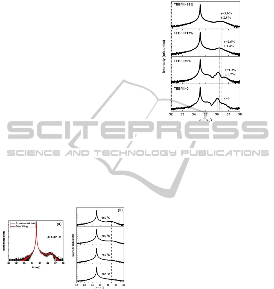
6.2.1 BAlN Thin Layers
Wurtzite BAlN layers with boron composition as
high as 12% were successfully grown by MOVPE.
The growth was performed at 650˚C and then
annealed at 1020˚C. Under high TEB/III ratio of
39%, as shown in Fig. 6(a), BAlN single layer
grown on GaN templates at 650˚C with 20 nm
thickness demonstrates an X-ray diffraction peak at
36.38˚ ( 0.17˚), which indicates that the layer has
smaller lattice c than AlN due to boron substituting
Al atoms in the crystal structure. We can assume the
layer is fully-relaxed considering the large lattice
mismatch between BAlN layer and GaN template. In
this case, the c-lattice constant is 4.935 Å ( 0.022
Å), which corresponds to boron composition of
5.6% ( 2.8%) by applying Vegard’s Law. The
complete relaxation of the layer can be confirmed in
Fig. 7: when we stop TEB flow and only grow AlN
layer, the 2θ-ω peak of the layer is located at 36.02˚
corresponding to completed relaxed AlN layer.
When the deposition temperature is increased,
shown in Fig. 6(b), the BAlN peak is weakened, and
then disappears when it is increased to 800˚C. It
indicates that under this high TEB/III ratio the
crystallinity is worse when the layer is grown at
higher temperature. Low temperature growth can
alleviate B-rich phase poisoning issue under high
TEB/III ratio.
Figure 6: (a) HR-XRD 2θ-ω scan of 20 nm BAlN layers
grown on GaN template at 650 °C under TEB/III=39%; (b)
shows the influence of growth temperature which was
varied between 650°C to 800°C.
In order to have different amount of boron
incorporation, a series of samples were grown on
GaN templates by continuous method, and TEB/III
ratio was changed run to run. As shown in Fig. 7,
when TEB/III ratio is increased from 0 to 39%, the
peak of the layer shifts gradually towards greater
diffraction angles (0 to 5.6% boron). The peak is
Figure 7: HR-XRD 2θ-ω scans of 20 nm BAlN grown on
GaN templates by continuous method under different
TEB/III ratio.
broadened with fringes missing due to
polycrystalline nature of BAlN.
BAlN single layers with clear defined X-ray
diffraction peaks were also achieved by flow-
modulate method on AlN templates which are
appropriate substrates for deep UV devices, as well
as on GaN templates in order to distiguish the XRD
peak of BAlN from the substrate peak. As shown in
Fig. 8, clear XRD peaks can be identified at 36.59˚
( 0.20˚) on both GaN and AlN templates. Lattice c
is 4.908 Å ( 0.025 Å) and the corresponding boron
content is 9% ( 3.2%). Since BAlN peak is very
close to AlN template peak, the deconvolution of
substrate peak and layer peak is shown in the inset
figure.
The concentration calculated by XRD has a large
error range because of the broadness of the BAlN
diffraction peak and uncertainty of the lattice
parameters and strain. These all influence
calculation of the composition from diffraction peak
positions, especially for the layer with high boron
content. So the boron incorporation into the layer
was also analysed by SIMS profile along the growth
direction in Fig. 9. The Al signal is decreased in the
BAlN layer compared with the signal of the template
indicating that boron atoms were substitutionally
incorporated into AlN lattice. Boron has a uniform
distribution along the growth direction. The
concentration of boron can be calculated based on
atomic concentration obtained by SIMS. In order to
calibrate the SIMS signal for quantitative
measurements, a boron-implanted AlN sample with
PHOTOPTICS2015-DoctoralConsortium
32
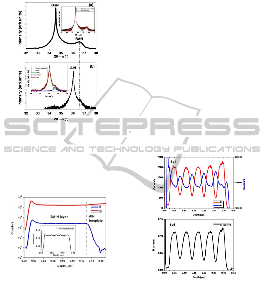
Figure 8: HR-XRD of 70 nm BAlN on (a) GaN template
and (b) AlN template by FME growth (TEB/III=39%).
Inset figures show the smoothing and deconvolution of
two peaks.
known boron content was used as a reference. The
concentration of boron calculated from the SIMS
signal is 12% with 0.6% error (inset of Fig. 9),
which agrees with the composition range given by
XRD diffraction peak positions (6% ~12%).
Figure 9: SIMS elemental concentration depth profiles of
B and Al for the sample grown on AlN template; inset
shows the boron concentration obtained by using boron
implanted AlN as calibration sample.
More details can be found in (X. Li, Sundaram, El
Gmili, et al. 2014). The promising results advance
prospects for MOVPE-grown boron alloys, which
can result in more freedom in bandgap, strain
engineering with tailoring of refractive index of
DBR structures for eventual deep-UV sources.
6.2.2 BAlN Heterostructure
Low temperature growth can alleviate the boron
poisoning issue, but it does not facilitate AlN growth
for the heterostructure. The fabrication of the
heterostructure is an important issue which needs to
be further developed no matter for BAlGaN-based
MQWs or for DBRs. In this subsection, 5-period
AlN/BAlN heterostructure was grown at 1000˚C.
Flow-modulate method was applied during BAlN
growth.
The boron concentration in the BAlN layers
along growth direction was evaluated by SIMS
profile, as shown in Fig. 10(a). It was clear that B
profile varies anti-phase with Al, which indicates
that Boron atoms substitute Al atoms on the III sites
of lattice to form alloy. 5-period AlN/BAlN layers
exhibit good uniformity except that the first AlN
layer has lower AlN intensity which is due to some
Ga contamination from the sample holder and the
reactor (Kim et al. 2014). The boron content
distribution along the growth direction was
presented in Fig. 10(b). Under our growth conditions,
11% ( ± 0.6%) boron incorporation has been
obtained.
Figure 10: (a) SIMS elemental concentration depth
profiles of B and Al for the sample grown on GaN
template; (b) Boron content in solid layers calculated from
SIMS by using boron implanted AlN sample as reference.
In order to investigate structural quality of this
heterostructure and also crystalline characteristics,
the cross-section STEM was performed along <1 1 -
2 0> zone axis. As shown in Fig. 11(a), the bright-
field STEM image shows that the AlN/BAlN
heterostructure has columnar polycrystalline features,
such as the part in the rectangle box. By looking into
BAlGaN-basedVerticalCavitySurfaceEmittingLaserOperatinginDeepUVRegion
33
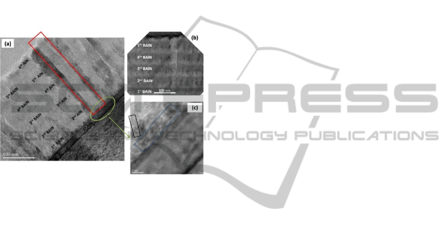
the higher magnification image of the interface
between 1
st
AlN and 1
st
BAlN in Fig. 11(c), it is
clear that the 1
st
AlN layer is still monocrystalline.
When BAlN growth starts, the lattice is oriented
along c-axis for around 5 nm, and then the tilt as
large as 60˚ can be observed which means the
structure tends to be polycrystalline and columnar
growth starts. Better contrast of AlN and BAlN
layers can be observed by Z-contrast HAADF-
STEM image shown in Fig. 11(b), where layers with
higher brightness represent AlN layers and darker
layers represent BAlN.
Figure 11: (a) STEM images (bright field) of 5-period
AlN/BAlN heterostructure and columns are clearly
observed in the structure; (b) HAADF-STEM image to
show better contrast of BAlN and AlN layers; (c) high
magnification of the zone where the 1
st
BAlN layer start to
grow.
The polycrystalline feature was caused by the short
diffusion length of boron atoms, which would
challenge the applications of this material. From
STEM image, we observed that the monocrystalline
critical thickness for BAlN with 11% boron is
around 5 nm, above which the polycrystalline
growth occurs. Meanwhile, the monocrystalline
critical thickness is around 500 nm for BAlN
containing 2% boron as reported in the literature
(Akasaka & Makimoto 2006). The more boron is
incorporated, the smaller monocrystalline thickness
of BAlN is. Therefore, for different applications, a
compromise can be achieved between thickness and
boron composition. For example, for deep UV DBRs,
boron incorporation no more than 5% is enough to
achieve high refractive index contrast (Watanabe et
al. 2003; Abid et al. 2012). So the boron content can
be decreased to maintain BAlN layers (30~40nm)
monocrystalline. For ultra-thin layers such as
MQWs or strain engineering superlattices, high
boron incorporation can be used allowing a large
design freedom and it can still be kept as
monocrystalline for its thin thickness (below 10 nm).
More details can be found in (X. Li, Sundaram,
El Gmili, et al. 2014).
6.3 Next Plans
Based on the preliminary results obtained, the next
steps would involve:
1. Design and realization of BAlN/AlGaN DBRs
with reflection at 280 nm. DBRs with high
boron content and polycrystalline feature will
be grown firstly. Then low boron would be
used in order to reduce the interface and
surface roughness. Meanwhile, AlGaN/AlN
DBRs would also be optimized as a reference.
2. Fabrication and tests of final laser devices
including laser diodes, RC-LEDs and VCSELs.
ACKNOWLEDGMENT
This work is supported by French ANR (Agence
Nationale de la Recherche) in the framework of
VESUVE project (ANR-11-BS03-0012). The
authors would like to thank David Troadec from
IEMN in Lille for FIB preparation.
REFERENCES
Abid, M. et al., 2012. Distributed Bragg reflectors based
on diluted boron-based BAlN alloys for deep
ultraviolet optoelectronic applications. Applied
Physics Letters, 100(5), p.051101.
Akasaka, T. & Makimoto, T., 2006. Flow-rate modulation
epitaxy of wurtzite AlBN. Applied Physics Letters,
88(4), p.041902.
Akasaki, I. et al., 1995. Stimulated emission by current
injection from an AlGaN / GaN / GaInN quantum
well device. Japanese Journal of Applied Physics, 34,
p.1517.
Bogusławski, P., Rapcewicz, K. & Bernholc, J.J., 2000.
Surface segregation and interface stability of
AlN/GaN , GaN/InN , and AlN/InN {0001} epitaxial
systems. Physical Review B, 61(16), pp.820–826.
Chuang, S.L. & Chang, C.S., 1996. KP Method for
strained wurtzite semiconductors. Physical Review B,
54(4), pp.2491–2504.
Ding, J. et al., 1990. Laser action in the blue-green from
optically pumped (Zn,Cd)Se/ZnSe single quantum
well structures. Applied Physics Letters, 57(26),
pp.2756–2758.
G.B.Stringfellow, 1993. Compositional ordering in
semiconductor alloys. Mater. Res. Soc. Symp. Proc.,
312, pp.35–46.
PHOTOPTICS2015-DoctoralConsortium
34

Gautier, S. et al., 2007. GaN materials growth by MOVPE
in a new-design reactor using DMHy and NH3.
Journal of Crystal Growth, 298, pp.428–432.
Gil, B., 1998. Group III nitride semiconductor compounds,
Clarendon Press.
Han, J. et al., 1998. AlGaN/GaN quantum well ultraviolet
light emitting diodes. Applied Physics Letters, 73(12),
p.1688.
Higuchi, Y. et al., 2008. Room-temperature CW lasing of
a GaN-based vertical-cavity surface-emitting laser by
current injection. Applied Physics Express, 1,
p.121102 1–3.
Hirayama, H. et al., 2007. 231–261 nm AlGaN deep-
ultraviolet light-emitting diodes fabricated on AlN
multilayer buffers grown by ammonia pulse-flow
method on sapphire. Applied Physics Letters, 91(7),
p.71901.
Hirayama, H. et al., 2014. Recent progress and future
prospects of AlGaN-based high-efficiency deep-
ultraviolet light-emitting diodes. Japanese Journal of
Applied Physics, 53(10), p.100209.
Ippommatsu, M. et al., 2013. Development of AlGaN
DUV-LED. In 10th Conference on Lasers and
Electro-Optics Pacific Rim (CLEO-PR).
Ivanov, S.V. et al., 2014. Plasma-assisted molecular beam
epitaxy of Al(Ga)N layers and quantum well
structures for optically pumped mid-UV lasers on c-
Al
2
O
3
. Semiconductor Science and Technology, 29(8),
p.084008.
Johnson, N.M. et al., 2012. In paper presented at the 9th
International Symposium on Semiconductor Light
Emitting Devices, Berlin.
Kasahara, D. et al., 2011. Demonstration of blue and
green GaN-based vertical-cavity surface-emitting
lasers by current injection at room temperature.
Applied Physics Express, 4(7), p.072103 1–3.
Kim, J. et al., 2014. Origins of unintentional incorporation
of gallium in InAlN layers during epitaxial growth,
part II: Effects of underlying layers and growth
chamber conditions. Journal of Crystal Growth, 388,
p.143-149.
Kolbe, T. et al., 2010. Optical polarization characteristics
of ultraviolet (In)(Al)GaN multiple quantum well
light emitting diodes. Applied Physics Letters, 97(17),
p.171105.
Krestnikov, I.L. & Ledentsov, N.N., 1999. Photopumped
InGaN / GaN / AlGaN Vertical Cavity Surface
Emitting Laser Operating at Room Temperature.
phys. stat. sol., 511, pp.511–516.
Leroux, M. et al., 2004. About some optical properties of
Al
x
Ga
1−x
N /GaN quantum wells grown by molecular
beam epitaxy. Superlattices and Microstructures, 36,
pp.659–674.
Leroux, M. et al., 2002. Optical characterization of
Al
x
Ga
1-x
N alloys ( x<0.7 ) grown on sapphire or
silicon. Physica Status Solidi (b), 234(3), pp.887–891.
Li, X., Sundaram, S., Disseix, P., et al., 2015. AlGaN-
based MQWs grown on a thick relaxed AlGaN buffer
on AlN templates emitting at 285 nm. Optical
Materials Express, 5(2), pp.380-392.
Li, X., Sundaram, S., El Gmili, Y., et al., 2014. BAlN thin
layers for deep UV applications. In E-MRS Spring
Meeting.
Li, X., Sundaram, S., El Gmili, Y., et al., 2014. MOVPE
grown periodic AlN/BAlN heterostructure with high
boron content. Journal of Crystal Growth, pp.3–6.
Li, X.-H. et al., 2014. Low-threshold stimulated emission
at 249 nm and 256 nm from AlGaN-based multiple-
quantum-well lasers grown on sapphire substrates.
Applied Physics Letters, 105(14), p.141106.
Lin, B.C. et al., 2014. Design and fabrication of a InGaN
vertical-cavity surface-emitting laser with a
composition-graded electron-blocking layer. Laser
Physics Letters, 11(8), p.085002.
Martens, M. et al., 2014. Performance characteristics of
UV-C AlGaN-based lasers grown on sapphire and
bulk AlN substrates. IEEE Photonics Technology
Letters, 26(4), pp.342–345.
McIntosh, F.G. et al., 1996. Growth and characterization
of AlInGaN quaternary alloys. Applied Physics
Letters, 68(1), p.40.
Mitrofanov, O. et al., 2006. High-reflectivity ultraviolet
AlGaN⁄AlGaN distributed Bragg reflectors. Applied
Physics Letters, 88(17), p.171101.
Moe, C.G. et al., 2006. AlGaN/AlN distributed bragg
reflectors for deep ultraviolet wavelengths. Physica
Status Solidi (a), 203(8), pp.1915–1919.
Murotani, H. et al., 2011. Silicon concentration
dependence of optical polarization in AlGaN
epitaxial layers. Applied Physics Letters, 98(2),
p.021910.
Nam, K.B. et al., 2004. Unique optical properties of
AlGaN alloys and related ultraviolet emitters.
Applied Physics Letters, 84(25), pp.5264–5266.
Northrup, J.E. et al., 2012. Effect of strain and barrier
composition on the polarization of light emission
from AlGaN/AlN quantum wells. Applied Physics
Letters, 100(2), p.021101.
Pantzas, K. et al., 2012. Nanometer-scale, quantitative
composition mappings of InGaN layers from a
combination of scanning transmission electron
microscopy and energy dispersive x-ray spectroscopy.
Nanotechnology, 23(45), p.455707.
Redwing, J.M. et al., 1996. An optically pumped GaN–
AlGaN vertical cavity surface emitting laser. Applied
Physics Letters, 69(1), pp.1–3.
Reuters, B. et al., 2012. Relaxation and critical strain for
maximum In incorporation in AlInGaN on GaN
grown by metal organic vapour phase epitaxy.
Journal of Applied Physics, 112(9), p.093524.
Ryu, H.-Y. et al., 2013. Investigation of light extraction
efficiency in AlGaN deep-ultraviolet light-emitting
diodes. Applied Physics Express, 6, p.062101.
Shatalov, M. et al., 2012. AlGaN deep-ultraviolet light-
emitting diodes with external quantum efficiency
above 10%. Applied Physics Express, 5, p.082101.
Shatalov, M. et al., 2002. Deep ultraviolet light-emitting
diodes using quaternary AlInGaN multiple quantum
wells. IEEE Journal of Selected Topics in Quantum
Electronics, 8(2), pp.302–309.
BAlGaN-basedVerticalCavitySurfaceEmittingLaserOperatinginDeepUVRegion
35

Tersoff, J., 1996. Stress-driven alloy decomposition during
step-flow growth. Physical review letters, 77(10),
pp.2017–2020.
Venezuela, P. et al., 1999. Self-organized growth of alloy
superlattices. Letters to nature, 397, pp.678–681.
Watanabe, S. et al., 2003. Refractive indices of B
x
Al
1−x
N
(x= 0-0.012) and B
y
Ga
1−y
N (y= 0-0.023) epitaxial
layers in ultraviolet region. Physica Status Solidi (c),
0(7), p.2691-2694.
Xie, J. et al., 2013. Lasing and longitudinal cavity modes
in photo-pumped deep ultraviolet AlGaN
heterostructures. Applied Physics Letters, 102(17),
p.171102.
PHOTOPTICS2015-DoctoralConsortium
36
