
A Sub-1V Bandgap Voltage Reference with Improved PSRR Scheme
Anass Slamti and Zakia Lakhliai
Computer and Interdisciplinary Physics Laboratory (L.I.P.I.), USMBA, Fez, Morocco
Keywords: Bandgap reference, power supply rejection ratio, temperature coefficient, error amplifier.
Abstract: A High performance sub-1V bandgap voltage reference (BGVR) with high power supply rejection ratio
(PSRR) and low temperature coefficient (TC) is proposed in this paper. An improved PSRR scheme is
inserted to isolate the supply voltage of the error amplifier and the supply voltage of BGVR core from a
power supply source in order to achieve a high PSRR. The proposed circuit is designed and simulated in
0.18μm CMOS 1.8V/3.3V technology. The proposed BGVR deliver an output voltage of 0.6346V at 27°C
and the measurement temperature coefficient is 22,3ppm/°C over temperature range -40°C to 140°C, the DC
value of PSRR is -93dB at 10kHz and -71dB of PSRR is achieved at 1MHz and a line regulation of
104μV/V is achieve over supply voltage range 1.2V to 1.8V. The area of layout is 0.0337 mm
2
. The
proposed sub-1V bandgap voltage reference is suitable for low power LDO regulators and switching
regulators.
1 INTRODUCTION
Bandgap voltage reference is a circuit used to
generate a fixed voltage, V
REF
, that in theory is
independent of the power supply voltage V
DD
(where
V
REF
<V
DD
), temperature, and process variations. In
other words, the ideal reference voltage is
independent of PVT. Voltage reference is among the
most important subcircuit in analog integrated
circuits and is used as an internal voltage reference
in linear regulator (LDO), switching regulator,
analog-to-digital converter (ADC) and digital-to-
analog converter (DAC) and other analog integrated
circuits. This is achieved by adding a voltage, which
is proportional to the absolute temperature (PTAT),
to a base-emitter voltage of diode connected Bipolar
Junction Transistor (BJT) NPN or PNP type which
is a complementary to the absolute temperature
(CTAT) in order to compensate for its first-order
temperature dependency (Razavi, 2017).
The classical design of BGVR circuits
commonly has an output voltage V
REF
around 1.25V
(close to the theoretical 1.206V bandgap
voltage of silicon at 0 K) (Widlar, 1971; Kujik,
1973; Brokaw, 1974; Tzanateas et al., 1979; Song
and Gray, 1983).
As the technology scales less than 350
nanometers, so do to supply voltages. The supply
voltages recently tend to be in the range of 0.6-1.2V.
The supply voltage scales with the technology, but
the threshold voltage of the transistors does not scale
at the same rate. This makes it difficult to
incorporate conventional design of bandgap voltage
reference to operates properly in the low supply
voltages. For the low voltage bandgap reference
design many approaches have been proposed;
resistive divider networks (Banba et al., 1999; Leung
and Mok, 2002; Ker et al., 2006), Current summing
and a voltage summing circuits (Ripamonti et al.,
1999), transimpedance amplifier (Jiang and Lee,
2000), dynamic threshold mosfets (Annema, 1999).
Other circuits have been proposed for the design of
sub-1V BGVR to have a low temperature coefficient
and at the same time a high PSRR (Andreou et al.,
2012; Xin et al., 2009), but they have always limited
by the short channel effects existing in nanometer
technologies which has a very low supply voltage,
and especially in the design of the opamp with very
low input offset voltage which remains an important
element in the BGVR circuit to provide a precise
voltage (or current) proportional to the absolute
temperature V
PTAT
(or I
PTAT
) because a very low
offset guarantees the obtaining of this voltage (or
this current).
This work propose a novel design for sub-1V
bandgap voltage reference generator while provide
an output voltage reference V
REF
with low TC and
high PSRR and good line regulation. In section 2,
Slamti, A. and Lakhliai, Z.
A Sub-1V Bandgap Voltage Reference with Improved PSRR Scheme.
DOI: 10.5220/0009772701850193
In Proceedings of the 1st International Conference of Computer Science and Renewable Energies (ICCSRE 2018), pages 185-193
ISBN: 978-989-758-431-2
Copyright
c
2020 by SCITEPRESS – Science and Technology Publications, Lda. All rights reserved
185
the conventional scheme of the sub-1V bandgap
voltage reference is analyzed to show the limits of
its performance. In section 3 a related work of high
PSRR structure of bandgap voltage reference is
presented. In section 4, the scheme of the proposed
circuit is given and a detailed analysis of BGVR
core generator is presented and the literal expression
of the output voltage reference is established in
order to show the design method of this block, also
the small high frequency signal model of the
proposed circuit is presented in order to calculate the
lateral expression of the PSRR. In section 5, the
simulation results are given to show the performance
of the proposed circuits and a comparison with
related works is presented. Finally in section 6 a
conclusion is given to show the contribution of the
proposed circuit.
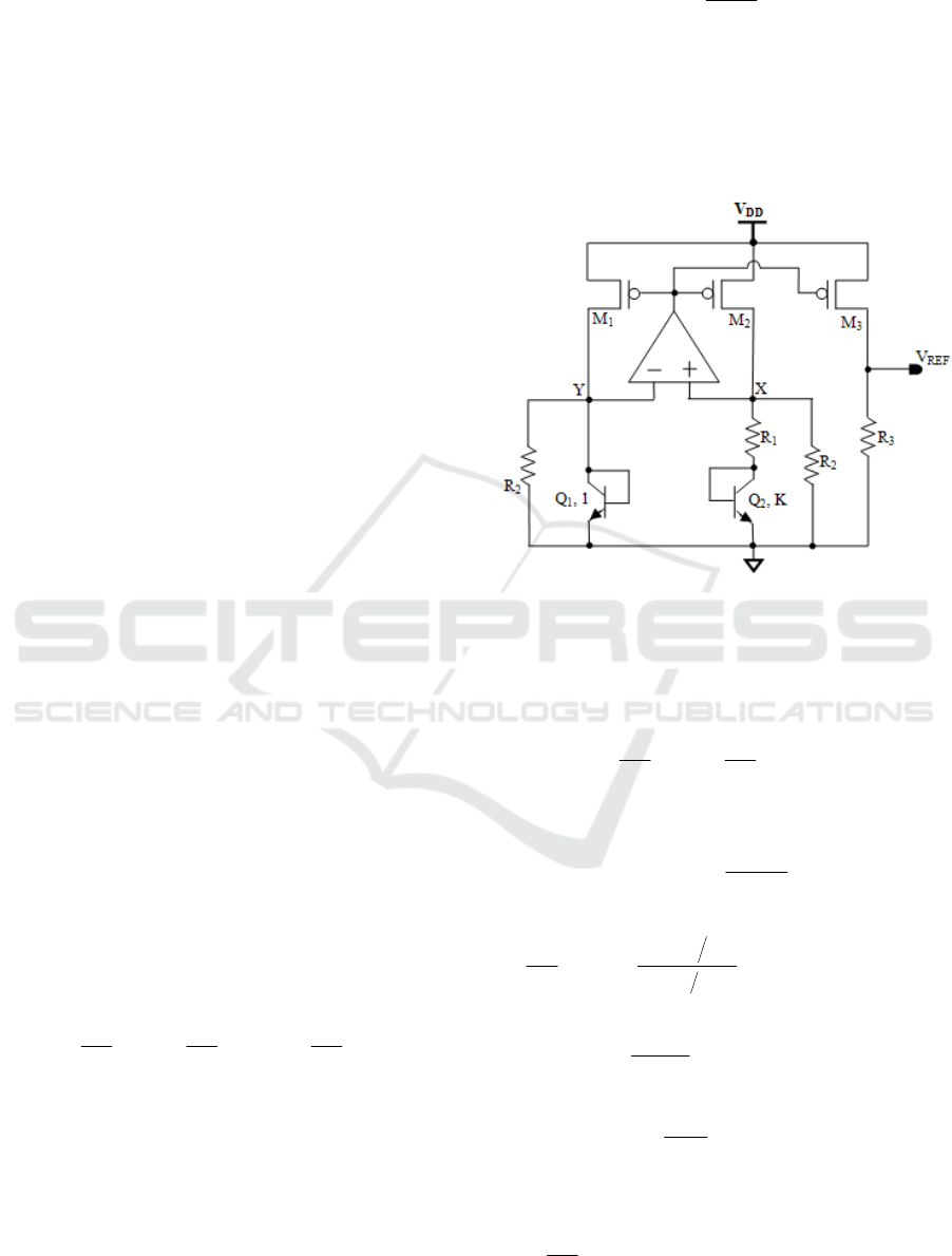
2 CONVENTIONAL SUB-1V
BANDGAP VOLTAGE
REFERENCE
The conventional sub-1V bandgap voltage reference
suitable for low power supply is shown in Figure 1
(Banba et al., 1999). He use an opamp based β-
multiplier architecture with resistive division, where
an opamp works as an error amplifier will form an
inverted feedback loop to enforce the two input
nodes X and Y of the opamp having the same
voltages.
The current mirror is formed by the PMOS
transistors M
1
, M
2
and M
3
having identical size, such
that the currents flowing through this three
transistors are the same. The β-multiplier consists of
two diode connected NPN transistors Q
1
and Q
2
,
with their emitter area ration being 1:K to provide
the required temperature dependent voltages to
construct the voltage reference circuit.
The output voltage reference V
REF
is expressed
as:
)V
R
R
V.lnK.
R
R
.(V
R
R
V
OS
1
2
T
1
2
BE
2
3
REF
1
(1)
Where,
1
BE
V
is the base-emitter voltage of BJT
Q
1
witch it’s had a negative temperature coefficient
and represents the CTAT voltage.
And V
T
is the thermal voltage (V
T
=25,9mV at
300K) expressed as,
q
T.k
V
B
T
(2)
Where k
B
is the Boltzmann’s Constant
(k
B
=1,381.10
-23
J.K
-1
), q is the electron’s charge
(q=1,602.10-19C) and T is the absolute temperature.
V
OS
present the input offset voltage of the
opamp.
Figure 1: Schematic of Conventional sub-1V BGVR.
V
T
has a positive temperature coefficient and
represents the PTAT voltage. If we neglect the value
of V
OS
, the Equation 1 becomes:
)V.lnK.
R
R
.(V
R
R
V
T
1
2
BE
2
3
REF
1
(3)
A voltage reference independent of the absolute
temperature is obtained if 0
T
V
REF
, then:
TV
TV
lnK.
R
R
T
BE
1
2
1
(4)
Noted that
0
T
V
1
BE
and its value depends on
the CMOS technology used and can be extracted by
simulation, while 0
T
V
T
and it value can easily
calculated.
The value of K is usually set to 8, so the resistor
ratio
1
2
R
R
can be calculated from Equation 4.
ICCSRE 2018 - International Conference of Computer Science and Renewable Energies
186
For a fixed value of V
REF
less than 1V, the value
of the resistance R
3
can be obtained from the
Equation 3. Noted that the V
REF
can be scaled by the
resistor ratio
2
3
R
R
, and thus achieve an arbitrary
V
REF
.
The conventional sub-1V BGVR using opamp β-
multiplier architecture ensures a low temperature
coefficient for V
REF
but remains very limited in
terms of PSRR caused by the input offset voltage
problem of the error amplifier, although some
modifications have been proposed to improve the
PSRR.
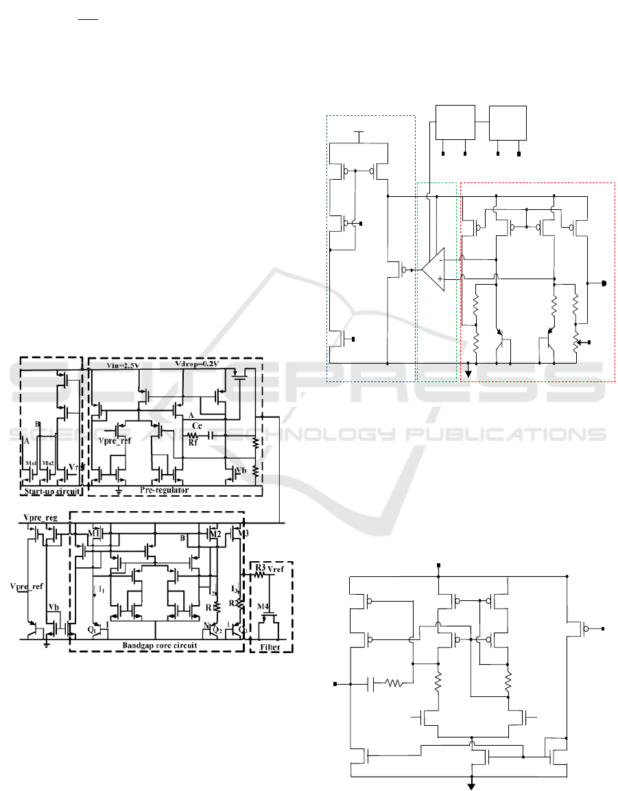
3 RELATED WORK
In order to achieve a high PSRR of the bandgap
voltage reference, a pre-regulator scheme and low
pass filter are added to a main circuit as shown in
Figure 2 (Li and Zhang, 2014). The pre-regulator
bloc improves a DC PSRR at low frequencies while
the low pass filter improves a little the value of
PSRR at high frequencies.
Figure 2: High PSRR structure of bandgap voltage
reference proposed in (Li and Zhang, 2014).
The disadvantage of this structure is the use of large
resistor to achieve a high PSRR and a low
temperature coefficient.
4 PROPOSED SUB-1V BANDGAP
VOLTAGE REFERENCE
The schematic of proposed sub-1V BGVR is shown
in Figure 3. A current mode regulator scheme is
inserted to improve the performance of the PSRR by
isolating a supply voltage of the error amplifier and
supply voltage of the BGVR core from a power
supply source VDD.
Figure 3: Schematic of proposed sub-1V BGVR
The schematic of the error amplifier used is
shown in Figure 4, a self biased cascode current
mirror load is adopted to achieve a high gain (Allen
and Holberg, 2002). This opamp need a network
compensation to achieve a sufficient phase margin to
guarantee closed-loop stability.
Figure 4: Schematic of error amplifier and his Bias circuit
M
7
M
6
M
5
M
21
M
8
V
bp
V
bn
R
2
V
REF
M
1
M
2
M
4
M
3
Q
1
, K
Q
2
R
1
R
2
R
3
R
3
OA
V
REG
V
bp
Startup
Circuit
Bias
Circuit
V
bp
V
DD
V
G6,7
V
REG
V
G6,7
V
bp
V
bn
Improved PSRR stage:
Current mode regulator
OpAmp
BVR generator core
V
G5
Y
X
M
11
M
20
M
12
M
14
M
15
X
V
REG
V
bp
M
16
M
13
Y
C
C
M
10
M
9
M
19
M
18
M
17
R
Z
V
bn
R
B
R
B
V
G5
A Sub-1V Bandgap Voltage Reference with Improved PSRR Scheme
187
Figure 5: Schematic of Start-up circuit
The supply voltage of the opamp is V
REG
which
equal to regulate source-drain voltage of M
5
. The
proposed sub-1V BGVR needs a start-up circuit
shown in Figure 5 to fix at the proper operation
point.
4.1. Analysis and Design of Proposed
BGVR Core
The core of the proposed BGVR uses the same
principle of the conventional scheme with some
modifications on the resistive voltage divider in
order to compensate the error introduced by the
input offset voltage of the error amplifier and
consequently to have the same voltage level in the X
and Y nodes.
The PMOS transistors M
1
, M
2
, M
3
and M
4
have
identical size, such that the currents flowing through
this four transistors are the same as
DDDD
IIII
321
. The β-multiplier consists of
two diode connected PNP transistors Q
1
and Q
2
,
with their emitter area ratio being K:1 to provide the
required temperature dependent voltages to construct
the voltage reference circuit.
The expression of the output voltage reference
V
REF
is given by:
)V.
R2
R
lnK.U.
R2
R
.(VKV
OS
1
2
T
1
2
EBRREF
2
(5)
With,
32
3
R
R2R
R2
K
(6)
lnK).U.
R2
R
.(VKV
T
1
2
EBRREF
2
(7)
If we take into account the input offset voltage
V
OS
, we have V
X
=V
Y
+V
OS
,
Thus the expression of V
REF
becomes:
)V.
R2
R
lnK.U.
R2
R
.(VKV
OS
1
2
T
1
2
EBRREF
2
(8)
Equation 9 shows that the factor amplifying the
input offset voltage is reduced in half in proposed
circuit compared to that of the conventional scheme
(see equation 1).
Differentiating equation 8 with respect to
absolute temperature yields:
)
T
V
.lnK.
R2
R
T
V
.(K
T
V
T
1
2
EB
R
REF
2
(9)
To achieve a near-zero TC of V
REF
, 0
T
V
REF
.
Thus,
TV
TV
lnK.
R2
R
T
EB
1
2
1
(10)
For the CMOS technology used in our design,
CmV/1.89
T
V
2
EB
, and by using Equation 2, we
have
CmV/0.0862
q
k
T
V
BT
, from where we
get:
9.21lnK.
R2
R
1
2
(11)
The value of K is close to 8, thus:
12
R.21R (12)
The value of R
1
is calculated from the following
equation:
PTAT
T
1
I
lnK.U
R
(13)
A reasonable current I
PTAT
is designed to bias
transistor Q
1
in the active region. The value of R
3
is
ICCSRE 2018 - International Conference of Computer Science and Renewable Energies
188

calculated from Equation 7 for a desired output
voltage reference V
REF
.
Design resistor example:
I
PTAT
=10μA,
V0.6V
2
EB
, V
REF
=0.65V.
We have:
PTAT
T
1
I
lnK.U
R
We get: R
1
=5.4 kΩ
From equation 12, we obtain: R
2
=113.4 kΩ.
From equation 6 and 7, we have:
)U21.(V
V
K
TEB
REF
R
2
We get: K
R
≈0.56
Frome equation 6, we obtain: R
3
=0.64.R
2
Thus: R
3
=72.6 kΩ
Note that the final values of the resistances
calculated by the hand must be adjusted during the
design of the circuit to obtain an optimal value of the
temperature coefficient of V
REF
over the required
temperature range.
The minimum supply voltage to ensure proper
operation of the proposed circuit and obtain an
output voltage reference V
REF
less than 1 V with a
small variation in the required temperature range is
such that the following two constraints are met:
6,7sat3,4sat
SDSDREFDD
VVVV (14)
And,
6,7sat1,2sat
SDSDEBDD
VVVV
2
(15)
Where
3,4sat
SD
V is the overdrive voltage of M
3
and M
4
,
1,2sat
SD
V is the overdrive voltage of M
1
and
M
2
and
6,7sat
SD
V is the overdrive voltage of M
6
and
M
7
.
4.2. PSRR Analysis
In order to reduce noise from the supply voltage
which directly influences the performance of the
PSRR, a pre-regulation stage is added to isolate the
supply voltage V
DD
from the supply voltage of the
operational amplifier and also the supply voltage of
the BGVR core generator.
To establish the expression of the PSRR, the
high frequency small signal model of the proposed
circuit is realised (see Figure 6). For the calculation
of the PSRR, a similar method to that adopted in
(Giustolisi and Palumbo, 2003) is applied. The body
effect is ignored and both Q
1
and Q
2
BJT transistors
can be considered as short-circuited.
The voltage v
dif
shown in Figure 5 is the small
signal part of the differential input voltage of the
opamp.
We have:
(s)v
(s)v
PSRR(s)
ref
dd
(16)
Where v
dd
(s) is the high frequency small signal
part of V
DD
, v
ref
(s) is the high frequency small signal
part of V
REF
and s is the complex variable of
Laplace.
We can write that:
(s)v
(s)v
(s)v
(s)v
PSRR(s)
ref
reg
reg
dd
(17)
Where v
reg
(s) is the high frequency small signal
part of V
REG
.
For a simple notation the variable s is omitted in
the voltages symbols.
Figure 6: High frequency small signal model of proposed
sub-1V BGVR
A Sub-1V Bandgap Voltage Reference with Improved PSRR Scheme
189

In the node D
3
, the Kirchhoff’s Current Law
gives:
ref
1
21131d
1
2reg3m
v).RY(Yv.Rv).Y(g
3
(18)
Where,
s.CgY
3ds033
(19)
s.CRY
3gd
1
311
(20)
v
d1
is the high frequency small signal part of V
D1
.
In the node D
1
, Kirchhoff’s Current Law gives:
ref
1
2011
1
2
reg
1
2011
1m
1d
v.
)RY(Y
R
v.
)RY(Y
)Y(g
v
1
(21)
Where,
s.CgY
1ds011
(22)
s.CRY
1gd
1
110
(23)
By substituting equation 21 in equation 18, we
obtain:
(s)D
(s)N
v
v
1
1
ref
reg
(24)
Where,
)Y.(gR)RY).(YY(g(s)N
11m
1
2
1
210133m1
(25)
)Y.(YR)RY).(YY(Y(s)D
111
1
2
1
21011131
(26)
In the node D
6
, the Kirchhoff’s Current Law
gives:
dd65mref31d14d4reg4
v).Y(gv.Yv.Yv.Yv(s).N
5g5gs5m6g6gd6m
vs)..C(gvs)..C(g
(27)
Where,
s]).CC(CYYgY[g(s)N
45gs6gd655mTmT4
(28)
4m3m2m1mmT
ggggg
(29)
4321T
YYYYY
(30)
s.CgY
2ds022
(31)
s.CgY
4ds044
(32)
s.CgY
5ds055
(33)
s.CgY
6ds046
(34)
4bs3bs2bs1bs4gs3gs2gs1gs4
CCCCCCCCC
(35)
And, v
d4
is the high frequency small signal part
of V
D4
, v
g5
is the high frequency small signal part of
V
G5
and v
g6
is the high frequency small signal part of
V
G6
.
In the node D
4
, the Kirchhoff’s Current Law gives:
reg
91
4m
4d
v.
)Y(Y
)Y(g
v
4
(36)
Where,
s.C)//R(RY
4gd
1
329
(37)
In the node G
5
, Kirchhoff’s Current Law gives:
1d
5gs5gdoutout
v
5g
v.
s]).C(C.[Yr
A
v
reg
5gs5gdout
5gs
v.
s]).C(C[Y
s.C
(38)
Where,
s.CrY
out
1
outout
(39)
A
v
is the open-loop gain of the opamp and r
out
is
its output resistance.
C
out
is all capacitance connected from the output
of the opamp to ground.
In the node G
6
, the Kirchhoff’s Current Law
gives:
reggddd1ggd1b
v.Cv.s.Cvs].).C(C[Y
666
888 sm
v).Y(g (40)
Where, v
s8
is the high frequency small signal part
of V
S8
and,
s.CRY
8gd
1
bb
(41)
ICCSRE 2018 - International Conference of Computer Science and Renewable Energies
190

Where R
b
represent the output resistance of
current source bias network and,
7bs6bs7gs6gs1
CCCCC
(42)
s.CgY
3088
(43)
7gd8ds3
CCC
(44)
In the node S
8
, the Kirchhoff’s Current Law
gives:
dd
2788m
77m
s
v.
s).CYY(g
)Y(g
v
8
6g
2788m
7m8
v.
s).CYY(g
)g(Y
(45)
Where,
8ds8gs2
CCC
(46)
By substituting equation 45 in equation 40, we
obtain:
reg
2
3
dd
2
2
g
v.
(s)D
(s)N
v.
(s)D
(s)N
v
6
(47)
Where,
s).CYYs(g.C(s)N
2878m12
)Y).(gY(g
77m88m
(48)
s).CYYs(g.C(s)N
2878m6gd3
(49)
s).CYYs)].(g).C(C[Y(s)D
2788m6gd1b2
)Y).(gY(g
78m87m
(50)
By substituting equations 21, 36, 38 and 47 in
equation 27, we obtain:
(s)]D(s)D(s)D(s)[D(s)D
(s)D(s).D(s).Ns)..CYg(g
v
v
87654
1326gd66m5m
dd
reg
(51)
Where,
(s)D(s).D(s).D(s).N(s)D
21344
(52)
(s).D(s).D(s)D
315
s).C(s).(gN
)Y(Y
)Y.(gY(s).D
5gd6m3
94
44m42
(53)
.r).Y.(gY(s).D(s).D(s)D
out11m1216
s]).C(C[Y
45gdout
(54)
s)..C(s).(gD(s).D(s)D
45m217
s].C).RY.(Yr)Y.(g[A
4
1
2101out11mv
(55)
(s).D(s).N(s)D
218
1
2v45m3345gdout
1
21out
R.As)..C(g(s)D.Ys]).C(C.[YR.Y.r
(56)
Note that g
0i
represents the small signal source-
drain conductance of the MOSFET M
i
and Y
i
represents the equivalent admittance for the shunt
connection of the impedance of the capacitor and a
resistor.
By substituting equations 24 and 51 in equation
17, we obtain:
(s)]D(s)D(s)D(s)[D(s)D
(s)N(s).D(s).Ns)..CYg(g
PSRR(s)
87654
1326gd66m5m
(57)
The expression of the PSRR(s) shows that its
transfer function has 7 poles and 7 zeros, and
consequently the frequency response is convergent
and the proposed circuit system is stable.
The expression of DC value (zero frequency) of
the PSRR is obtained by replacing s=0 in all the
terms containing the complex variable s. Thus,
)]0(D)0(D)0(D)0([D)0(D
)0(N).0(D).0(N).gg(g
)0PSRR(
87654
132066m5m
(58)
The equation 58 shows that the DC value of
PSSR can be improved by more than 20dB in
comparison to the previous high PSRR structures in
related work (Li and Zhang, 2014; Tham and
Nagaraj, 1995; Francisco and Hora, 2012).
5 SIMULATION RESULTS AND
LAYOUT
The proposed design of sub-1V bandgap voltage
reference was simulated in 0.18-μm CMOS
1.8V/3.3V technology using Cadence Virtuoso
Spectre Simulator. The proposed circuit generates an
output voltage reference V
REF
of 0.6346 V at 27°C
when the supply voltage is set to 1.8V. As it is
shown in Figure 7, the measurement temperature
coefficient of V
REF
is 22,3ppm/°C over temperature
range -40°C to 140°C.
A Sub-1V Bandgap Voltage Reference with Improved PSRR Scheme
191
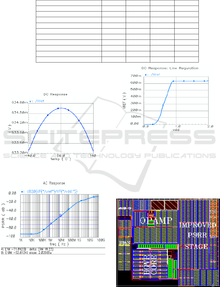
As it is shown in Figure 8 the DC value of PSRR is
-93dB at 10 kHz and -71dB at 1MHz is achieved.
The measurement line regulation of V
REF
is
104μV/V as it is shown in Figure 9.
Figure 7: Simulated temperature dependence of the output
voltage reference at 1.8 supply voltage.
Figure 8: Simulated PSRR of the proposed sub-1V BGVR.
Figure 9: Simulated line regulation of the proposed sub-
1V BGVR.
Table 1 summarizes performance characteristics
of the proposed sub-1V BGVR and comparison with
related works is given. As shown in Table I, the
proposed circuit satisfied the high performance of a
voltage reference and especially for the PSRR value
in the 1MHz to 10MHz frequency range which is
significantly higher than the value found in the
related works (see Table 1).
Table 1: Simulation results summary and comparison
Performance [17] [18] [19] This work
Technology (CMOS) 0,9 μm 0.09 μm 0.18 μm 0.18 μm
V
DD,min
(V) 2.7 2.6 2.5 1.2
V
DD,max
(V) 5.5 3.6 6 1.8
V
REF
(V) 1.236 0.21398 1.194 0.6346
TC (ppm/°C) 85 6.07 6.51 22.3
Temperature operation range (°C) -50 to 125 -20 to 120 -25 to 80 -40 to 140
Line regulation 20μV/V 1143μV/V 104μV/V
PSRR DC (dB) -80 -82.7 -125 -93
PSRR@ 1MHz -40 -40 -71
PSRR@ 10MHz -52.8
ICCSRE 2018 - International Conference of Computer Science and Renewable Energies
192

Figure 10: Layout of proposed sub-1V BGVR reference
The layout of the proposed sub-1V bandgap
voltage reference is shown in Figure 10, the area is
0.0337 mm
2
.
6 CONCLUSIONS
In this paper a novel design of sub-1V bandgap
voltage reference circuit with opamp base β-
multiplier and resistive divider architecture is
proposed. The important contribution of this work is
the obtaining of an accurate voltage reference value
with a high value of the PSRR in a very wide
frequency range from 1kHz up to 10MHz.
The proposed architecture of the voltage divider
has made it possible to minimize the undesirable
effect of the input offset voltage of the opamp and
consequently to obtain a very accurate value of the
output voltage and to improve the dc value of the
PSRR.
In order to reduce noise from the supply voltage
which directly influences the performance of the
PSRR, a pre-regulation stage is added to isolate the
supply voltage source from the supply voltage of the
operational amplifier and also the supply voltage of
the BGVR core generator which allows improving
the value of the PSRR in high frequency.
REFERENCES
Razavi, B., 2017. Design of Analog CMOS Integrated
Circuits. McGraw-Hill Education. Los Angeles, 2
nd
edition.
Widlar, R.J., 1971. New Developments in IC Voltage
Regulators. IEEE Journal of Solid State Circuits,
Vol. SC-6, p 2-7.
Kujik, K.E., 1973. A precision reference voltage source.
IEEE Journal of Solid State Circuits, 8 (3) p 222-226.
Brokaw, A.P., 1974. A Simple three-terminal IC Bandgap
Reference. IEEE Journal of Solid State Circuits, 9 (6)
p 388–393.
Tzanateas, G., et al., 1979. A CMOS BG Reference. IEEE
Journal of solid-State Circuits, 14 (3) p 655-657.
Song, Bang-Sup and Gray, P., 1983. A Precision
Curvative-compensated CMOS BG Reference. IEEE
Journal of Solid State Circuits, 18 (6) p 634-643.
Banba, H., et al., 1999. A CMOS Bandgap Reference with
Sub-1-V Operation. IEEE Journal of Solid State
Circuits, Vol 34, pp. 670-674.
Leung, Ka Nang and Mok, P.K.T., 2002. Sub-1-V
15ppm/°C CMOS Bandgap Voltage Reference without
Requiring low Threshold Voltage Device. IEEE
Journal of Solid State Circuits, 37 (4), pp. 526-529.
Ker, M.D. et al., 2006. New Curvative-Compensation
Technique for CMOS Bandgap Reference with Sub-1-
V Operation. IEEE Journal of Solid State Circuits and
Systems-II:Express Briefs, 53 (8), pp. 667-671.
Ripamonti, G., et al., 1999. Low Power – Low Voltage
Bandgap Refrences for Flash EEPROM Integrated
Circuits: Design Alternatives and Experiments. In
Proceedings of ICECS 1999, Vol. 2, pp. 635-638.
Jiang, Yueming, and Lee, E.K.F., 2000. Design of Low-
Voltage Bandgap Refrence Using Transimpedance
Amplifier. IEEE Transactions on Circuits and
Systems-II, Vol. 47, pp. 552-555.
Annema, Anne-Johan, 1999. Low-Power Bandgap
References Future DTMOST’s. IEEE Journal of Solid
State Circuits, Vol 34, pp. 949-955.
Andreou, C.M., et al., 2012. A Novel Wide-Temperature-
Range, 3.9ppm/oC CMOS Bandgap Reference Circuit.
IEEE Journal of Solid-State Circuits, vol.47, no. 2, pp.
574–581.
Xin, Ming, et al., 2009. A 2.8 ppm/◦C high PSRR
BiCMOS bandgap voltage reference. Journal of
Semiconductors, Vol.30, No. 9.
Li, Xiuhan, and Zhang, Hanru, 2014. A High PSRR
Voltage Reference for High Efficiency Power
Management Circuits of MEMS Energy Harvesters,’’
Journal of Applied Science and Engineering, Vol. 17,
No.2, pp. 111-116.
Allen, Phillip E. and Holberg, Douglas R., 2002. CMOS
Analog Circuit Design. Oxford University Press. New
York, 2
nd
edition.
Giustolisi, G. and Palumbo, G. 2003. A Detailed Analysis
of Power Supply Noise Attenuation in Bandgap
Voltage References. IEEE Transactions On Circuits
and System-I: Fundamental Theory and Applications,
vol. 50, No. 2, p. 185-197.
Tham, Khong-Meng and Nagaraj, K., 1995. A Low
Supply Voltage High PSRR Voltage Reference in
CMOS Process. IEEE Journal of Solid State Circuits,
vol. 30, No. 5, pp. 586-590.
Francisco, Keith R. and Hora, Jefferson A., 2012. Very
Low Bandgap Voltage Reference With High PSRR
Enhancement Stage Implemented in 90nm CMOS
Process Technology for LDO Application. IEEE
International Conference on Electronics Design
Systems and Applications.
A Sub-1V Bandgap Voltage Reference with Improved PSRR Scheme
193
