
Surface Structure and Morphology of Gallium Nitride Thin Film
Grown on Molybdenum Disulfide Layer
by Molecular Beam Epitaxy
Iwan Susanto
1,2
, Ing-Song Yu
1
, Dianta Mustofa Kamal
2
, Belyamin
2
, Fuad Zainuri
2
,
Sulaksana Permana
2,3
, Chi-Yu Tsai
1
, Yen-Ten Ho
4
, Ping-Yu Tsai
5
1
Department of Materials Science and Engineering, National Dong Hwa University, Hualien 97401, Taiwan ROC
2
Department of Mechanical Engineering, State Polytechnic of Jakarta, Depok 16424, Indonesia
3
Center of Mineral Processing and Corrosion Research, Department of Metallurgy and Materials Engineering,
University of Indonesia, 16424 Depok, Indonesia
4
International College of Semiconductor Technology, National Chiao Tung University, Hsinchu 300, Taiwan ROC
5
Department of Electronic Systems Research Division, Chung-Shan Institute of Science & Technology,
Tao-Yan 325, Taiwan ROC
belyamin@mesin.pnj.ac.id, fuad.zainuri@mesin.pnj.ac.id, sulaksana@yahoo.com
Keywords: Gallium Nitride, Thin Films, Molybdenum Disulfide, Surface Character
Abstract: The layer of gallium nitride thin film was grown near to the surface of the molybdenum disulfide substrate
by plasma-assisted molecule beam epitaxy (PA-MBE) system. In-situ RHEED and ex-situ characterization
of AFM and SEM were used to exploit subsequently the surface character of GaN films. The results show
that the RHEED pattern demonstrated the mix structure of polycrystalline and amorphous with 2-
dimensional (2D) growth mode. The crystalline structure was influenced by the defect constructed in the
GaN films. Meanwhile, the 3D AFM image served in detail the smooth surface with root mean square
(RMS) of 3.87 nm. Further, the SEM image with an EDS pattern performed the fixture of morphology and
surface composition. However, Ga cluster like particles presented on the surface of the GaN layer. The
sufficient of the thermal energy with the crystalline structure provided by the substrate would be a
promising approach for creating GaN film with greater structures and smoother surface.
1 INTRODUCTION
GaN semiconductor is an interesting material
because it has several excellent properties like high
electrons mobility, high conductivity and chemically
stable (Kawashima et al., 1997; Hanada, 2009).
According to this feature, GaN was utilized for some
applications of optoelectronic devices and electronic
components (Würtele et al., 2011; Su, Chen and
Rajan, 2013; Joshin et al., 2014; Chen et al., 2017).
Unfortunately, GaN layers are generally grown on
other materials substrate, since the GaN bulk has
been a high-cost material as subtract (Liu and Edgar,
2002). Several attempts have been done for growing
GaN layers on other materials (Kukushkin et al.,
2008). However, the lattice-mismatched with
different thermal expansion coefficient rises the
residual stress which could create defects in GaN
film during the cooling process (Trampert, 2002;
Poust et al., 2003). In general, the defects will be
started from the surface boundary in the interface of
two materials and afterward they propagate to the
inside of the film up to the surface of GaN film
(Trampert, 2002).
Several efforts have been strived for reducing the
residual strain by growing the GaN layer on the
close-lattice matched (Mánuel et al., 2010; Gupta et
al., 2016) (Susanto, C.-Y. Tsai, et al., 2019).
Recently, MoS
2
as an interesting semiconductor
material applied for optoelectronic which is grown
on GaN material (Wan et al., 2018; Zhang et al.,
2018). Since the MoS
2
has been a lattice-matched
with closed to GaN, it becomes a promising chance
for growing high-quality GaN film layers.
Moreover, GaN films are usually grown with a thick
layer until 1.8 µm (Kimura et al., 2005), So that the
Susanto, I., Yu, I., Kamal, D., Belyamin, ., Zainuri, F., Permana, S., Tsai, C., Ho, Y. and Tsai, P.
Surface Structure and Morphology of Gallium Nitride Thin Film Grown on Molybdenum Disulfide Layer by Molecular Beam Epitaxy.
DOI: 10.5220/0009871000002905
In Proceedings of the 8th Annual Southeast Asian International Seminar (ASAIS 2019), pages 27-30
ISBN: 978-989-758-468-8
Copyright
c
2022 by SCITEPRESS – Science and Technology Publications, Lda. All rights reserved
27

defects were not seen on the surface of the film. On
the other hand, observations of the GaN film surface
near the substrate surface have also not been
reported more clearly. It will be an interesting
section to investigate the thin layer near to the
surface substrate which has a potential area to
generate serious defects at the surface boundary.
So, in this study, we investigated the surface
structure and morphology of GaN grown near to the
surface of the MoS
2
layer by molecular beam
epitaxy technique. The surface of the substrate and
GaN film was observed using in-situ and ex-situ
characterization techniques. Observation of two
surfaces is carried out using RHEED, AFM, and
SEM. The results of the characterization will be
presented in 2-dimensional (2D) and 3-dimensional
(D) images. Structure and character of the surface
will be analyzed using the results of RHEED
monitoring. Whereas surface roughness will be
monitored using AFM. Meanwhile, the morphology
and composition of surface elements will be
investigated by SEM.
2 EXPERIMENTAL METHOD
The GaN layer was grown on the MoS
2
substrate
using the PA-MBE system. While, the substrate used
to deposit the MoS
2
layer is a single crystal of c-
plane sapphire by the PLD method (Ho et al., 2015).
The deposited temperature was given at 800 C with
a background pressure at 8 x 10⁻⁶ Torr. For GaN
film, the growth temperature is determined at 600 C
for 20 minutes with a substrate rotation speed of 10
rpm. All of the growth parameters have been done in
our previous study (Susanto, C. Tsai, et al., 2019).
Before the growth process of the GaN layer, the
substrate is heated up to 600 for 40 minutes to clean
contaminants on the surface. The growth of the GaN
layer carried out using K-cell as a producer of Ga
atoms at 800 C and facilitated by a nitrogen gun as a
source of N atoms with a flow rate of 0.8 sccm at Rf
power 500 Watt. The ratio flux of nitrogen and
gallium (N/Ga) is 161 or N-rich conditions (Susanto
et al., 2017). During the cleaning substrate and
growth GaN film, the surface condition is monitored
using RHEED. Finally, the GaN film products were
then examined by AFM and SEM to investigate in
detail the characteristics of surface condition.
3 RESULT AND DISCUSSION
Figure 1 shows the RHEED pattern on the surface of
MoS
2
during the hot cleaning process. The foggy
pattern is shown by RHEED in Figure 1(a) before
hot cleaning. This pattern explains that the structure
formed of the MoS
2
layer is amorphous. After the
hot cleaning, a bright streak pattern is displayed by
RHEED in Figure 1 (b). This pattern explains that
the surface structure constructed on the MoS
2
layer
is a crystalline structure. So, based on the cleaning
results by the heating process, the surface structure
is changed from amorphous to crystalline. This
process was found to be effective in removing
contaminants that covered the surface of the MoS
2
layer and improving the surface structure of the
substrate. Besides, the striped pattern explains that
the surface layer is 2-dimensional. Meanwhile, the
bright intensity of the streak pattern shown explains
the crystal structure formed in the MoS
2
layer. The
stronger intensity of the pattern indicates the
crystallinity structure formed. Further, the RHEED
pattern in Figure 1 (c) displays the surface of the
GaN film growing on the MoS
2
layer. The dots
connected with a ring in the RHEED pattern show
the surface structure of the layer which is a
polycrystalline structure. This structure leads to be
constructed low mobilization of atoms caused by the
lack of heat energy provided by the substrate results
in the creation of Ga droplets or clusters due to low
desorption and diffusion of atoms (Susanto et al.,
2017). Moreover, the substrate's surface character
related to the different orientation was also
responsible for creating the structure. While the
weak intensity pattern correlates with the
polycrystalline mixed with an amorphous structure.
In addition, the single crystal of GaN films was not
constructed on the epitaxial structure. It indicates
that the defect was formed on the layer and
influencing the crystalline structure. The result is
consistent with the surface morphology on the GaN
film shown in the AFM image in Figure 1(d). The
peaks and valleys pattern on the surface illustrates
the surface character of the GaN film formed. The
RMS total of surface roughness constructed on GaN
film is 3.87 nm, in which the height peak is 118.93
nm and the depth valley is 15.99 nm. The presence
of peaks could be due to the accumulation of Ga
atoms which generate Ga clusters during the growth
process. The formation of valleys is created due to
the low mobilization of Ga and N atoms during
growth as well. The minimum of atoms mobilization
corresponds to less desorption influenced by the
ASAIS 2019 - Annual Southeast Asian International Seminar
28
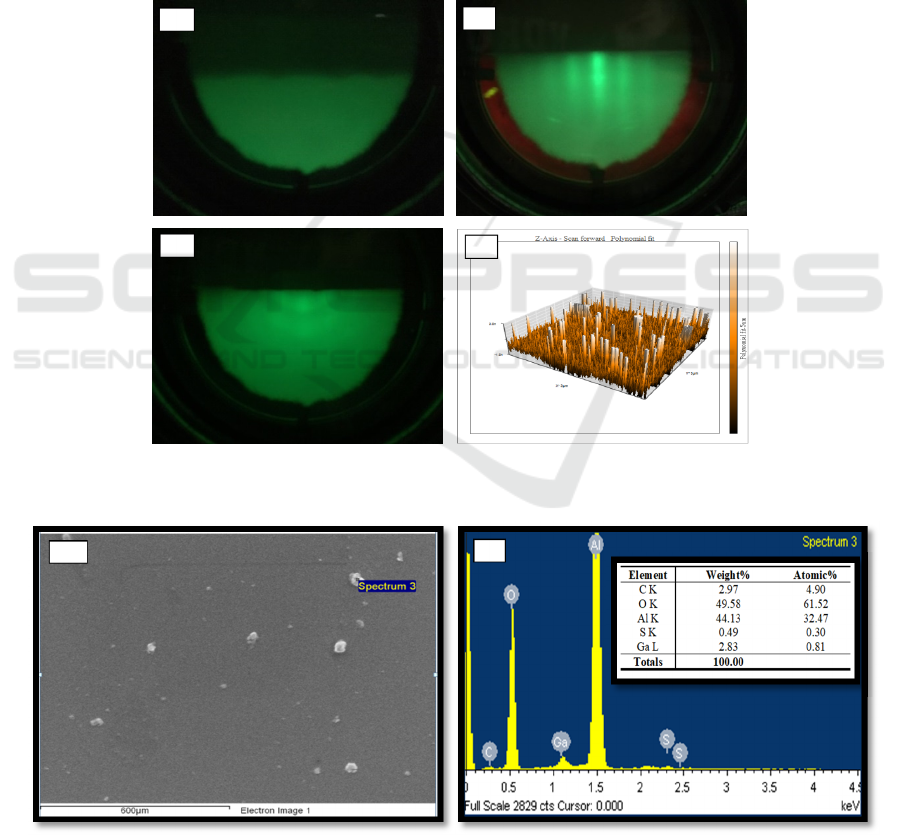
insufficiency of thermal energy (Susanto, Kan and
Yu, 2017).
Furthermore, the morphology and composition
element of the surface film was presented more
clearly in Figure 2. The GaN film with some light
particles has completely covered the substrate. The
smooth surface corresponded to 2D layers has
deposited on the MoS
2
layer. However, there are
also Ga clusters like a particle with a brighter color
attend on the surface of the GaN film. The clusters
pattern is believed to be the peaks demonstrated in
the AFM image in figure 1 (d). To ensure these
particles are Ga clusters, the observations are
targeted more focus at particles in spectrum 3 using
the EDS test shown in Figure 2(a). The result of the
spectrum 3 observations is shown in Figure 2 (b).
The peaks on the image are the elements constructed
from such as the films and substrate. The high peak
corresponds to the quality of the elements, while the
area of peaks relates to the number of elements.
Moreover, the number of elements namely Al, O, S,
C, and Ga is tabulated inset in Figure 2(b). The
presenting of Al, O and S elements could become
from the substrate material, while the Ga element
attends from Ga films. Based on the surface
morphology and composition element results, it
clears that the GaN film has grown well on the MoS
2
layer without the pits defect on the surface.
Figure 1: RHEED patterns (a) MoS
2
/Sapphire, (b) MoS
2
/Sapphire after nitridation, (c) GaN films, and (d) 3-dimensional
(3D) AFM GaN film surfaces with a volume of 3 µm x 3 µm x 5nm.
Figure 2. SEM and EDS images of GaN film surface
(a)
(b)
(c)
(d)
(b
(a)
Surface Structure and Morphology of Gallium Nitride Thin Film Grown on Molybdenum Disulfide Layer by Molecular Beam Epitaxy
29

4 CONCLUSIONS
The GaN layer has been successfully grown near the
surface of the MoS
2
layer with the PA-MBE
technique. The surface substrate of the MoS
2
layer
was covered throughout with GaN films. The
structure formed on the GaN film was either
polycrystalline closed-amorphous or a mixture
structures of polycrystalline and amorphous. The
defect influenced the crystalline structure of GaN
films. While the surface contour formed was in 2D
mode with a roughness of RMS 3.87. The smooth
layer of GaN film with presenting the Ga cluster also
constructed on the MoS
2
layer. The low heat energy
provided by the substrate was responsible to
construct the Ga cluster on the surface of GaN films.
In addition, the mixture of structures formed is also
believed to be formed due to low mobilization and
desorption of atoms during the growth epitaxy.
ACKNOWLEDGMENTS
All authors would like to thank Ministry of Science
and Technology, Taiwan for financially supporting
this study (MOST 107-2221-E-259- 001-MY2 and
107-3017-F-009-002), and Dr. Iwan Susanto would
like to give thanks for the support provided by Pusat
Penelitian dan Pengabdian Masyarakat, Politeknik
Negeri Jakarta (PPPM PNJ nomor
SP.DIPA.042.01.2.400994/2019).
REFERENCES
Chen, K. J. et al. (2017) ‘GaN-on-Si power technology:
Devices and applications’, IEEE Transactions on
Electron Devices. doi: 10.1109/TED.2017.2657579.
Gupta, P. et al. (2016) ‘Layered transition metal
dichalcogenides: promising near-lattice-matched
substrates for GaN growth’, Scientific Reports. doi:
10.1038/srep23708.
Hanada, T. (2009) ‘Basic Properties of ZnO, GaN, and
Related Materials’, in. doi: 10.1007/978-3-540-88847-
5_1.
Ho, Y. T. et al. (2015) ‘Layered MoS
2
grown on c -
sapphire by pulsed laser deposition’, Physica Status
Solidi - Rapid Research Letters, 9(3), pp. 187–191.
doi: 10.1002/pssr.201409561.
Joshin, K. et al. (2014) ‘Outlook for GaN HEMT
technology’, Fujitsu Scientific and Technical Journal.
Kawashima, T. et al. (1997) ‘Optical properties of
hexagonal GaN’, Journal of Applied Physics. doi:
10.1063/1.365671.
Kimura, R. et al. (2005) ‘Thick cubic GaN film growth
using ultra-thin low-temperature buffer layer by RF-
MBE’, Journal of Crystal Growth, 278(1–4), pp. 411–
414. doi: 10.1016/j.jcrysgro.2005.01.058.
Kukushkin, S. A. et al. (2008) ‘Substrates for epitaxy of
gallium nitride: New materials and techniques’,
Reviews on Advanced Materials Science.
Liu, L. and Edgar, J. H. (2002) ‘Substrates for gallium
nitride epitaxy’, 37, pp. 61–127.
Mánuel, J. M. et al. (2010) ‘Structural and compositional
homogeneity of InAlN epitaxial layers nearly lattice-
matched to GaN’, Acta Materialia. doi:
10.1016/j.actamat.2010.04.001.
Poust, B. D. et al. (2003) ‘SiC substrate defects and III-N
heteroepitaxy’, Journal of Physics D: Applied Physics.
doi: 10.1088/0022-3727/36/10A/321.
Su, M., Chen, C. and Rajan, S. (2013) ‘Prospects for the
application of GaN power devices in hybrid electric
vehicle drive systems’, Semiconductor Science and
Technology. doi: 10.1088/0268-1242/28/7/074012.
Susanto, I. et al. (2017) ‘Effects of N/Ga flux ratio on GaN
films grown on 4H-SiC substrate with 4° miscutting
orientation by plasma-assisted molecular beam
epitaxy’, Journal of Alloys and Compounds. Elsevier
B.V, 710, pp. 800–808. doi:
10.1016/j.jallcom.2017.03.320.
Susanto, I., Tsai, C., et al. (2019) ‘Morphology and
surface stability of GaN thin film grown on the short
growth time by Plasma Assisted Molecular Beam
Epitaxy’, J. Phs : Conference Seriese, 1364(012067).
doi: 10.1088/1742-6596/1364/1/012067.
Susanto, I., Tsai, C.-Y., et al. (2019) ‘The influence of 2D
MoS
2
layers on the growth of GaN films by plasma-
assisted molecular beam epitaxy’, Applied Surface
Science, 496(July), p. 143616. doi:
10.1016/j.apsusc.2019.143616.
Susanto, I., Kan, K. and Yu, I. (2017) ‘Temperature
effects for GaN fi lms grown on 4H-SiC substrate with
4 miscutting orientation by plasma-assisted molecular
beam epitaxy’, Journal of Alloys and Compounds.
Elsevier B.V, 723, pp. 21–29. doi:
10.1016/j.jallcom.2017.06.224.
Trampert, A. (2002) ‘Heteroepitaxy of dissimilar
materials: Effect of interface structure on strain and
defect formation’, in Physica E: Low-Dimensional
Systems and Nanostructures. doi: 10.1016/S1386-
9477(02)00317-X.
Wan, Y. et al. (2018) ‘Epitaxial Single-Layer MoS
2
on
GaN with Enhanced Valley Helicity’, Advanced
Materials. doi: 10.1002/adma.201703888.
Würtele, M. A. et al. (2011) ‘Application of GaN-based
ultraviolet-C light emitting diodes - UV LEDs - for
water disinfection’, Water Research. doi:
10.1016/j.watres.2010.11.015.
Zhang, Z. et al. (2018) ‘Interface Engineering of
Monolayer MoS
2
/GaN Hybrid Heterostructure:
Modified Band Alignment for Photocatalytic Water
Splitting Application by Nitridation Treatment’, ACS
Applied Materials and Interfaces. doi:
10.1021/acsami.8b01286.
ASAIS 2019 - Annual Southeast Asian International Seminar
30
