Design of High Gain Switched Capacitor Z-Source Converter with
Extended SC Cells
Kaveri Sanjeevreddy
1 a
and M. S. Aspalli
1 b
1
Department
of Electrical and Electronics Engineering (Affiliated to VTU Belgaum)
Poojya Doddappa Appa College of Engineering, Kalaburagi (Affiliated to VTU Belgaum), Karnataka, India
Keywords: Z Source Converter, Switched Capacitor Converter, High Gain Converter, Voltage Stress.
Abstract: In this paper, a switched capacitor-based z source converter is proposed and extended with switched capacitor
cells to further improve the voltage conversion ratio(1). The proposed converter minimizes the stress of the
power electronic switches and diodes less than that of half the load voltage and provides a high voltage
conversion ratio unaccompanied by any changes in the duty ratio and also minimizing the requirement of
passive or active components. The modes of operation of the converter is analysed and comparison of
proposed converter with similar structures of dc-dc converters are provided. The simulation work is carried
out in MATLAB/Simulink software. A hardware model is developed and the performance of the converter is
validated.
1 INTRODUCTION
Recently, greater focus has been placed on the
technological advancement of renewable energy
generation, such as Solar and wind energy. The low
voltage output of the solar panels is one of the primary
limitations of PV generating. To increase the Solar
panel voltage to values like 400 V in order to fulfil the
DC MG's voltage requirements, a converter with a
large voltage conversion ratio is needed. The PV
voltage can be increased using two usual methods:
pairing solar panels in series, or using a standard boost
converter. Because the entire system is affected if one
of the solar panels fails, the series connection is
unreliable. The typical boost converter offers
extremely high duty cycle and great voltage gain.
However, it frequently has serious output diode
reverse-recovery issues, low efficiency, and excessive
stress from voltage over the power electronic switches
and output diode. In order to increase the PV voltage
and get around the issues that the serial arrangement
of solar panels and the traditional boost converter
present, sophisticated high boost DC-DC converters
are being investigated (Habibi, S,2021). Due to the
extensive use of components,
________________________________
a
https://orcid.org/ 0009-0004-0499-2075
b
https://orcid.org/ 0000-0002-5483-6415
architectures constructed around SL and SC modules
are both expensive and complex. With a converter
constructed using coupled inductor or built in
transformer to hold onto the energy from inductance
leakage and lessen the strain caused by voltage across
the power switches, a clamping circuitry is necessary.
Recently, the idea of increasing voltage through quasi-
source (qZS) and Z-source (ZS)converter topologies
are being used. The voltage conversion ratio for
traditional ZS and (qZS) topologies, however, is
insufficient. A novel of higher boosting ZS converters
was created by integrating the SL technique into
traditional ZS network and was utilised as an input
phase of a two stage, 3ф Z-Source inverter. There are
many components and a duty cycle limit of 0.33, a
value below the threshold of 0.5 for the traditional ZS
topology, despite the voltage conversion ratio being
raised and voltage is contrasted to the traditional
similar topologies. The inclusion of the SC cells and
the traditional (qZS) network produced a novel
converter with a high voltage conversion ratio and
minimal voltage strain on the semiconductors
(Rahimi,2020).
In this paper, a new structure of Z Source converter
(Naser Vosoughi Kurdkandi,2020) is designed by the
integration of switched capacitor cells to the
traditional Z source impedance network, in order to
achieve high voltage conversion with reduced switch
voltage stress and minimum number of passive
components(Hu, X et al.,2020). The proposed
32
Sanjeevreddy, K. and Aspalli, M.
Design of High Gain Switched Capacitor Z-Source Converter with Extended SC Cells.
DOI: 10.5220/0012505900003808
Paper published under CC license (CC BY-NC-ND 4.0)
In Proceedings of the 1st International Conference on Intelligent and Sustainable Power and Energy Systems (ISPES 2023), pages 32-37
ISBN: 978-989-758-689-7
Proceedings Copyright © 2024 by SCITEPRESS – Science and Technology Publications, Lda.

converter topology eliminates the limitations on the
duty ratio. It is further extended by introducing the
switched capacitor cells controlled by an auxiliary
switch which further improves the voltage conversion
ratio without adding to the voltage stress.
2 SYSTEM DESCRIPTION
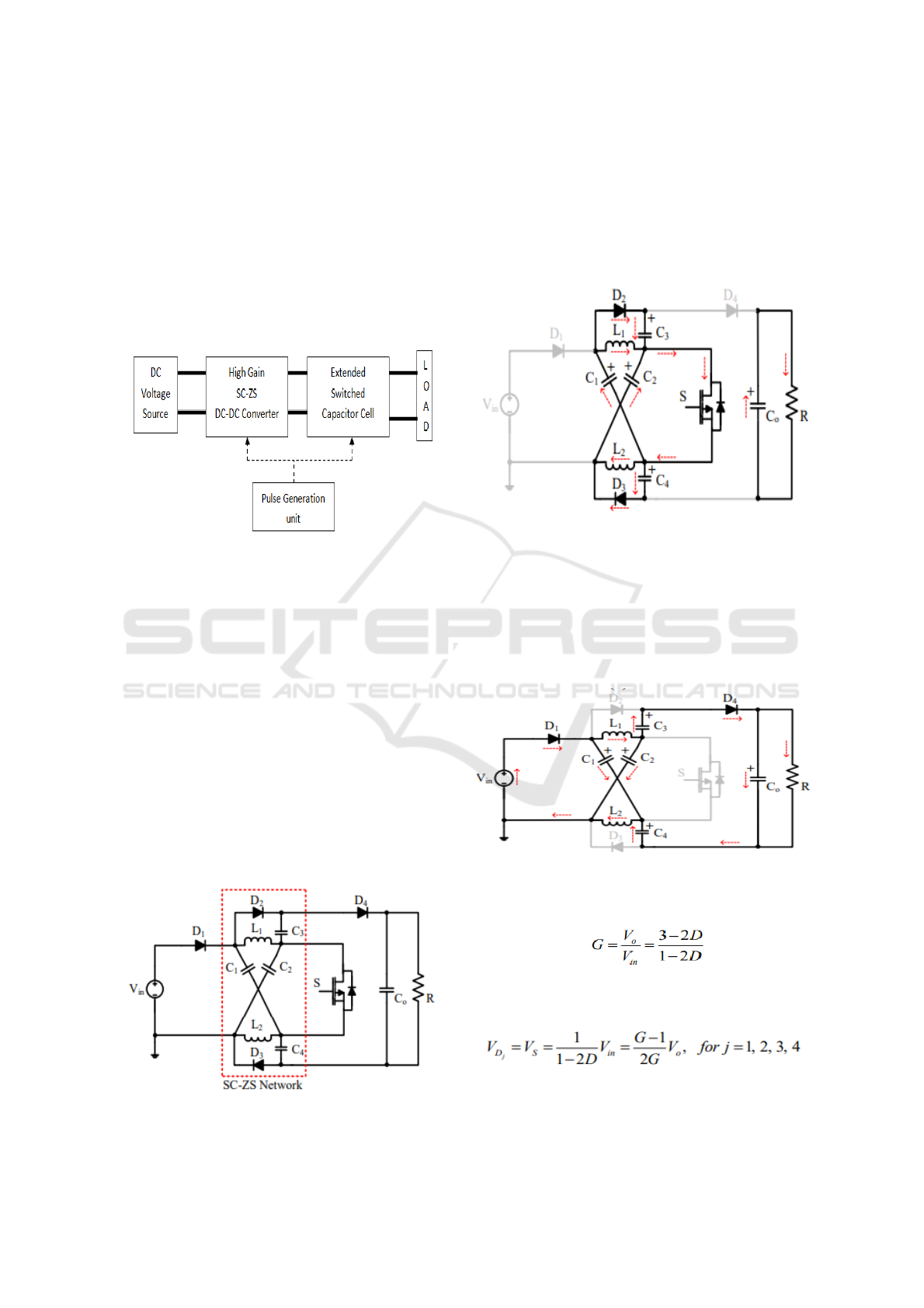
The proposed system is provided below in Fig 1.
Figure 1: Proposed system Block diagram.
The DC voltage source is connected to the
proposed converter which provides boosted voltage to
the load based on the pulse provided by the pulse
generation unit. The proposed converter is of two parts
switched capacitor-based Z Source converter and
extended SC cells so that the voltage conversion ratio
is improved.
The ZS DC-DC converter below is comprised of
single mosfet S with inductors (L1, L2), diodes (D1,
D2, D3, D4) and capacitors (C1, C2, C3, C4, Co). The
traditional ZS impedance network is coupled with
switched capacitor cells, a new impedance converter
is designed (SC-ZS converter) which possess a
symmetrical composition, improves the voltage
conversion ratio and also minimizes the switch
voltage stress across the diodes and power electronic
switch.
Figure 2: SC-ZS converter.
The operational stages of the above-mentioned
converter is provided below:
Stage 1:
When the switch is ON, the capacitors C1 and C2 are
discharging along with inductors L1 and L2. The
capacitors C3 and C4 are charging. The output
capacitance Co provides energy to the load.
Figure 2(a): Stage 1 operational circuit of SC-ZS converter.
Stage 2:
When the switch is OFF, the capacitors C1 and C2 are
charging along with inductors L1 and L2. The
capacitors C3 and C4 are discharging provides supply
to the load.
Figure 2(b): Stage 2 operational circuit of SC-ZS converter.
The voltage conversion ratio G is:
The voltage across the power electronic switch S and
diodes D1-D4 are calculated as:
Extended Switched Capacitor cell:
Design of High Gain Switched Capacitor Z-Source Converter with Extended SC Cells
33

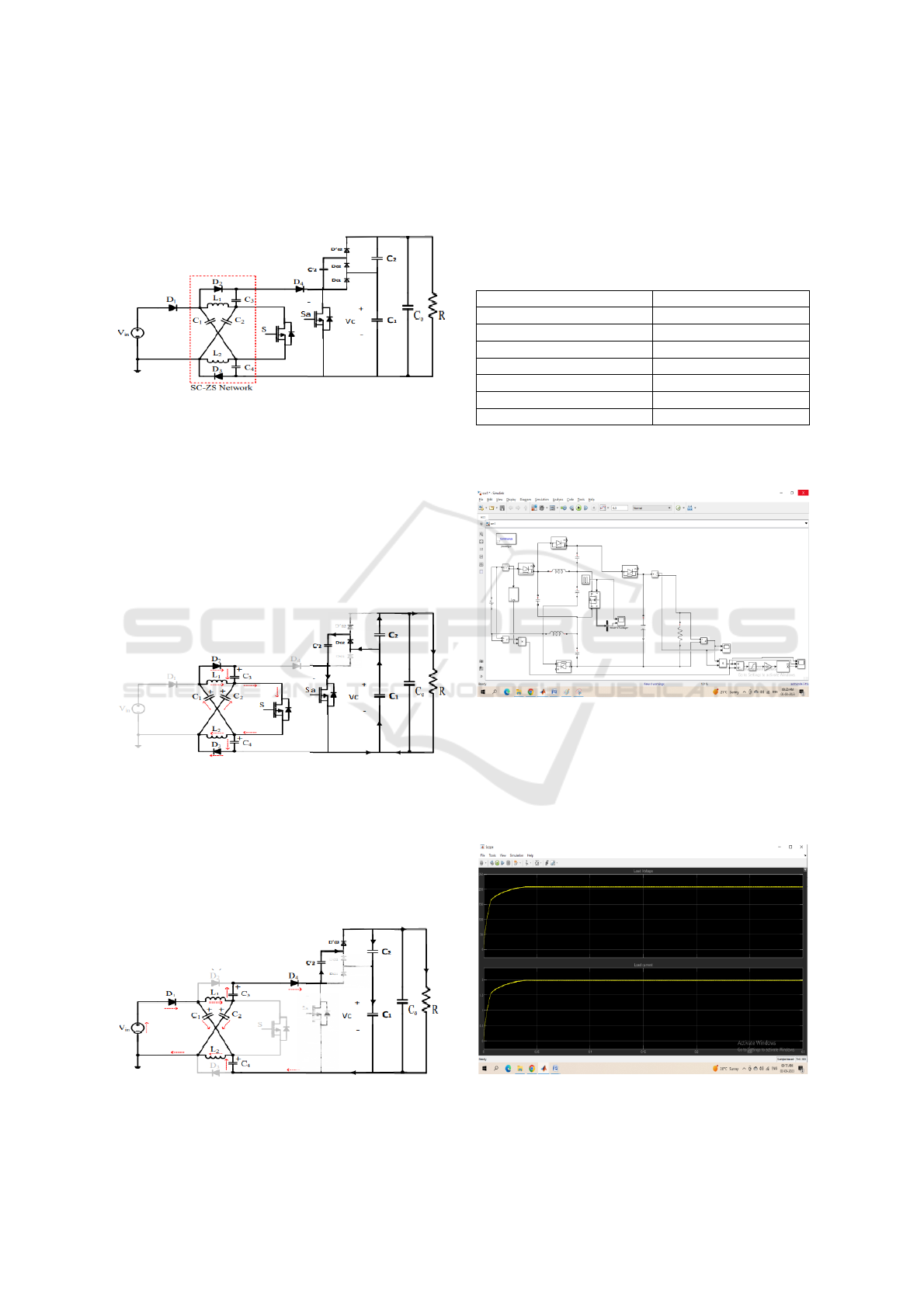
It is further extended by adding switched capacitor cell
with auxiliary switch to improve the voltage
conversion ratio without increasing the stress on the
diodes and power electronic switches.
Figure 3: Improved SC-ZS converter with extended SC
cells.
The operation of this proposed converter is same as
conventional SC-ZS converter for modes 1 and 2.
Stage 3:
In this, the capacitor C2 and C2’ are used to improve
the voltage conversion ratio. When the switch Sa is
ON, the C1 discharges and charges capacitor C2’
through the diode Do2. Diode Do2’ is reverse biased
where Do2 conducts.
Figure 3(a) Stage 3: operational circuit of proposed
converter.
Stage 4:
When the switch Sa is OFF, C2’ discharge and
provides energy to load along with C1 and C2. The
diodes Do1 and Do2 are reverse biased where Do2’
conducts.
Figure 3(b) Stage 4: operational circuit of proposed
converter.
3 SIMULATION SETUP &
RESULTS
The simulation parameters for the proposed converter
are shown below in Table 1.
Table 1: Simulation Parameters.
Input Voltage
12 V
Input power
450W
Switching Frequency
5 KHZ
Inductor
91.1mH
SC cell Capacitor
56µF
Output Capacitor
20mF
Load voltage
220V
Load Resistance
100 ohm
The simulation circuit of the high gain voltage
converter is provided below:
Figure 4: Simulation circuit of SC-ZS converter.
In this, the input voltage is provided as 12V and the
output voltage is designed for 220V. The duty ratio is
around 0.44 for gating pulse of 5KHz switching
frequency. The waveforms of the load voltage and
current is shown below:
Figure 5: Simulation Waveforms of load voltage and current
of SC-ZS converter.
ISPES 2023 - International Conference on Intelligent and Sustainable Power and Energy Systems
34

The load voltage is around 220V and current is 2A.
The switching gate pulse and the switch voltage stress
is provided below:
Figure 6: Gate Pulse and voltage waveforms of SC-ZS
converter.
The switch voltage is calculated as 104V and here
we achieve the switch voltage around 104.5V in
simulation of the high gain converter. The efficiency
of power curves of the converter is provided below:
Figure 7: Input Power, Load Power and %Efficiency
waveforms of SC-ZS converter.
Figure 8: Simulation circuit of the SC-ZS converter with
extended SC cells.
The input power is around 447W and load power
is around 415W with efficiency as 93.65%. The
extended cell is added to the high gain converter and
is given in figure 8.
In this, a switched capacitor cell is connected
along with the high gain converter and provides
supply to the load. The waveforms of load voltage and
current of the proposed converter is provided in
figure.9 The load voltage is around 275V and load
current is 2.6A for the same duty ratio of 0.44. The
voltage conversion ratio is further improved by 1.25
times than that of converter without extended
switched capacitor cell.
Figure 9: Simulation waveforms of Load voltage and current
of SC-ZS converter with extended SC cells.
Design of High Gain Switched Capacitor Z-Source Converter with Extended SC Cells
35

The efficiency of power curves of the converter is
provided below:
Figure 10: Input Power, Load Power and %Efficiency
waveforms of SC-ZS converter.
The input power is around 745W and load power
is around 700W with efficiency as 93.1%.
A hardware prototype model of proposed
converter with input voltage of 12V is developed with
output voltage of 220V with load resistance of 1KΩ.
The hardware parameters is provided below in the
following Table 2.
Table 2: Hardware Parameters.
Arduino uno control is used for generating the
pulses for the proposed converter and it is provided to
driver circuit (TLP 250) in order to drive the mosfets
IRF 250.
The load voltage is provided below:
Figure 11: The load voltage of the proposed converter is
around 240V with 100V/div in the above waveform.
Figure 12: Hardware Setup of proposed system.
4 CONCLUSIONS
In this paper, switched capacitor based z source
converter is designed and the operational modes of the
converter was analysed with extended switched
capacitor cells. The voltage stress of the switch was
calculated and verified with the simulation results.
The voltage conversion ratio of sc-zs converter was
18.33 and further improved by 1.25 times by adding
switched capacitor cells without any changes in duty
ratio. The efficiency of the proposed converter is
measured as 93.1% for the input power of 750W and
load of 100 ohm. A hardware prototype model was
developed and the operation of the proposed converter
is verified with the results.The main advantages and
applications of this proposed converter are, the
voltage gain can be increased without increasing the
pulse width and hence the voltage stress is kept lower.
ISPES 2023 - International Conference on Intelligent and Sustainable Power and Energy Systems
36

The voltage gain can be further extended by increasing
the switched capacitor cells compared to the literature
and It can be used for battery charging applications,
dc drives, renewable energy.
REFERENCES
Habibi, S., Rahimi, R., Shamsi, P., & Mehdi Ferdowsi.
(2021). Efficiency Assessment of a Residential DC
Nanogrid with Low and High Distribution Voltages
Using Realistic Data. ArXiv (Cornell University).
https://doi.org/10.1109/greentech48523.2021.0009.
Rahimi, R., Farhadi, M., Moradi, G. R., Farhangi, B., &
Farhangi, S. (2020). Filter-Clamped Two-Level Three-
Phase Transformerless Grid-Connected Photovoltaic
Inverter for Leakage Current Reduction. SSRN
Electronic Journal.
https://doi.org/10.2139/ssrn.3567399.
Naser Vosoughi Kurdkandi, Farhadi, M., Ebrahim Babaei,
& Pedram Ghavidel. (2020). Design and analysis of a
switched‐capacitor DC‐DC converter with variable
conversion ratio. International Journal of Circuit
Theory and Applications, 48(10), 1638–1657.
https://doi.org/10.1002/cta.2849
Hu, X., Liu, X., Zhang, Y., Yu, Z., & Jiang, S. (2021). A
Hybrid Cascaded High Step-Up DC–DC Converter
With Ultralow Voltage Stress. IEEE Journal of
Emerging and Selected Topics in Power
Electronics, 9(2), 1824–1836.
https://doi.org/10.1109/jestpe.2020.2975856
Rahimi, R., Habibi, S., Shamsi, P., & Mehdi Ferdowsi.
(2021). A Dual-Switch Coupled Inductor-Based High
Step- Up DC-DC Converter for Photovoltaic-Based
Renewable Energy Applications.
https://doi.org/10.1109/tpec51183.2021.9384916
Rahimi, R. (2021). An Interleaved High Step-Up DC-DC
Converter Based on Combination of Coupled Inductor
and Built-in Transformer for Photovoltaic-Grid Electric
Vehicle DC Fast Charging Systems. IEEE Texas Power
and Energy Conference (TPEC).
Kumar, P., & Mummadi Veerachary. (2021). Z-Network
Plus Switched-Capacitor Boost DC–DC
Converter. IEEE Journal of Emerging and Selected
Topics in Power Electronics, 9(1), 791–803.
https://doi.org/10.1109/jestpe.2019.2959078
Sreenu, S., Upendar, J., & Sirisha, B. (2022). Analysis of
switched impedance source/quasi-impedance source
DC-DC converters for photovoltaic
system. International Journal of Applied Power
Engineering (IJAPE), 11(1), 14.
https://doi.org/10.11591/ijape.v11.i1.pp14-24
Forouzesh, M., Siwakoti, Y. P., Gorji, S. A., Blaabjerg, F.,
& Lehman, B. (2017). Step-Up DC–DC Converters: A
Comprehensive Review of Voltage-Boosting
Techniques, Topologies, and Applications. IEEE
Transactions on Power Electronics, 32(12), 9143–9178.
https://doi.org/10.1109/tpel.2017.2652318
Design of High Gain Switched Capacitor Z-Source Converter with Extended SC Cells
37
