
Design of a SI Cuk Converter based on Bridgeless Power Factor
Correction with Regenerative Braking
Swaliyabegum Mulla
1 a
and M. S. Aspalli
1 b
Department of Electrical and Electronics Engineering (Affiliated to VTU Belgaum)
Poojya Doddappa Appa College of Engineering, Kalaburagi (Affiliated to VTU Belgaum), Karnataka, India
Keywords: Cuk Converter, Power Factor Correction, High Gain Converter, Regenerative Braking.
Abstract: The size of a switched inductor (SI) based Cuk converter is lowered with increased power factor when the
bridge is removed from an electric car charging system. The traditional techniques for battery charging
involve two-stage power conversion. The single stage switching inductor topology improves the voltage
conversion ratio. A high gain bidirectional converter is introduced to power the motor for the operation of an
electric vehicle after the performance of the converter under steady state and transient situations is noted.
Software called MATLAB/Simulink is used to carry out the simulation job. In order to verify that the
suggested system operates as intended, a hardware model is created.
1 INTRODUCTION
Given the constantly increasing share of demand for
LEVs, the charging station outfitted utilizing a
superior method for improving power quality is
highly anticipated from the perspectives of both
power distributors and users. The current generation
of LEV chargers frequently begin with a dc-dc
converter that is either isolated or not, together with a
configuration of an unregulated rectifier and a dc bus
capacitor. When DBR and a big dc-link capacitor are
used together, the input's power factor (PF) and
overall system efficiency all suffer because they draw
harmonics-rich distorted current from the supply.
Power factor correction (PFC) largely eliminates
these flaws in conventional low power rating
converters. In an APFC approach, a dc-dc converter
is employed between DBR and CDC to improve the
source side of the converter's performance from the
standpoint of power quality(Lachvajderova et
al,2021)(Wang et al,2021). It is crucial to understand
that an APFC conversion, whether it is a single-stage
converter or a two-stage converter with
differentconfigurations, can perform a variety of tasks
in a charger. In a two -stage setup, an APF cuk
________________________
a
https://orcid.org/0009-0001-4998-6785
b
https://orcid.org/0000-0002-5483-6415
converter is utilized to satisfy source requirements,
while a second dc-dc converter is required to satisfy
load requirements. In single-stage converters,
however, a single APF cuk converter fulfils both
criteria. A number of two-stage converter designs
based on various APFC techniques have been
researched for the purpose of charging EVs and
LEVs. Each technique has benefits and drawbacks in
terms of component tally, conductance and switch
losses, control complexity, and effectiveness. To
improve efficiency by reducing conduction losses on
the APF cuk conversion stage, several bridgeless
APFC converters with partial or complete deletion of
the DBR have been recorded in the literature. The
presentation includes a full investigation of bridgeless
APF cuk converters (Bahrami et al,2020). Certain
bridgeless integrated charging techniques have
recently been presented as a way to keep the
advantages of two-stage converters while reducing
the number of parts and inefficiencies in the chargers
(Dulau at al.,2020). Integration of the power
electronic equipment reduces the overall number of
devices and associated losses. However, the rising
control complexity and high device pressures account
for their diminished appeal for LEV applications. The
ripple-free charging current is one of the two-stage
converter's primary advantages. The performance of
the battery, as has been asserted by a number of
authors, is unaffected by low-frequency fluctuations
in the pushing current when they are properly
Mulla, S. and Aspalli, M.
Design of a SI Cuk Converter Based on Bridgeless Power Factor Correction with Regenerative Braking.
DOI: 10.5220/0012524900003808
Paper published under CC license (CC BY-NC-ND 4.0)
In Proceedings of the 1st International Conference on Intelligent and Sustainable Power and Energy Systems (ISPES 2023), pages 107-115
ISBN: 978-989-758-689-7
Proceedings Copyright © 2024 by SCITEPRESS – Science and Technology Publications, Lda.
107

regulated (Rachid et al., 2022). To address these
issues with two-stage converters, numerous
researchers have proposed alternate single-stage
converter topologies for EVs/LEVs together with
enhanced power quality at the source side. The single-
stage converters provide a low component count, high
power density, and an easy-to-understand control
design (Habib,2018). A properly designed single-
stage converter configuration may also provide
superior efficiency compared to its two-stage
converter. The common buck converter's high supply
current distortion at the zero crossing and the standard
boost converter's constrained output voltage
capabilities exclude their possible usage as an APFC
in single-stage LEV converters. The disadvantages of
buck and boost derived converters are therefore
typically eliminated when utilizing buck-boost
derived converters. The Cuk model of buck-boost dc-
dc converters has the least amount of output and input
current ripple. Traditional buck-boost dc-dc
converters, on the other hand, are less suitable to
provide a transformerless single-stage conversion for
the LEVs due to their low gain capabilities. Due to
the low battery voltage, the transformerless charger
architecture in LEVs operates at an extremely low
duty ratio, which eventually affects the charger's
dynamic efficiency and performance. The common
buck converter's high supply current distortion at the
zero crossing and the standard boost converter's
constrained output voltage capabilities exclude their
possible usage as an APFC in single-stage LEV
converters. The disadvantages of buck and boost
derived converters are therefore typically eliminated
when utilizing buck-boost derived converters. The
Cuk model of buck-boost dc-dc converters has the
least amount of output and input current ripple.
Traditional buck-boost dc-dc converters, on the other
hand, are less suitable to provide a transformerless
single-stage conversion for the LEVs due to their low
gain capabilities. Due to the low battery voltage, the
transformerless charger architecture in LEVs
operates at an extremely low duty ratio, which
eventually affects the charger's dynamic efficiency
and performance. Therefore, the majority of single-
stage LEV converters based on conventional dc-dc
converters require a transformer in order to achieve
the required dc voltage gain. However, the
transformer drives up the cost and size of the charger.
The leakage inductance of the transformer also
increases the voltage stress between the parts. The
transformerless charger architecture for LEVs based
on improved power quality is still seldom ever
discussed in academia. coupling inductors, converter
cascading, the use of multipliers, interleaved front
end structures, switched inductors, and hybrid
switched inductor-capacitor structures are recent
developments (Khalid et,2021) (Das et al,2021).
However, in the case of linked inductors, the coupling
coefficient has a significant impact on the operational
parameters of the converter. The quadratic converter
is more effective than a cascaded converter at
adjusting for increasing voltage and current stresses.
As a remedy to these issues, a switching dual network
composed of two to three diodes, split type inductors,
or capacitors is proposed. This charger is costly, has
a challenging control system, and has larger magnetic
components due to the CCM operation. This research
presents a single-stage Cuk converter-based modified
power factor improved converter. Because the dcm
mode of operation eliminates the need for sensors, the
controller design is straightforward. The converter's
bridgeless design results in a significant reduction in
the number of components used. The proposed
converter is put to the test using constant voltage and
constant current control techniques with variable
input voltage conditions. Once the vehicle is running
on battery power, the motor is powered via a high
gain bidirectional converter. Regenerative braking
can be used and extend the vehicle's running time
because of the bidirectional property.
2 SYSTEM DESCRIPTION
The proposed system is provided below in Fig 1.
Fig 1: Proposed system Block diagram.
The ac supply is connected to the BSIC converter
in this case while the car is charging so that the battery
can be charged while switch 1 (S1) is ON and switch
2 (S2) is OFF. The battery serves as the load in this.
The control loop regulates the voltage and current of
the battery. S1 is OFF (the ac source is disconnected)
and S2 is ON (the motor is connected) when the car
starts. The battery serves as the supply in this. The
measured speed of the DC motor is fed into the speed
ISPES 2023 - International Conference on Intelligent and Sustainable Power and Energy Systems
108
control loop, which regulates the output voltage of the
bidirectional converter, causing the measured speed
to match the reference speed.
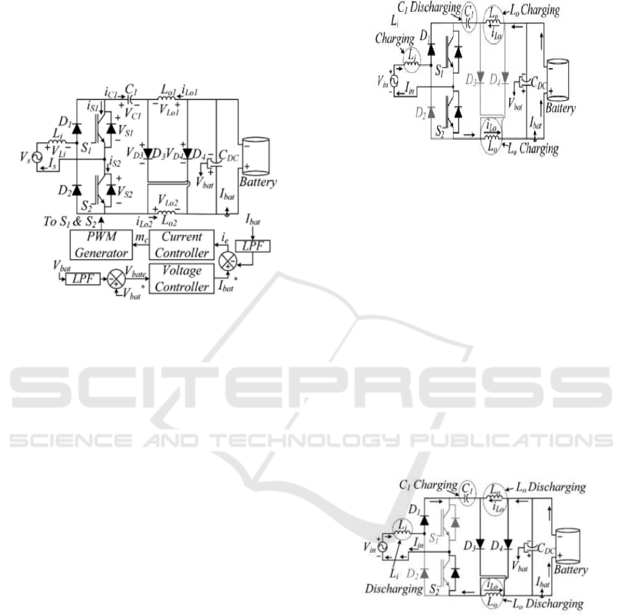
2.1 BSIC Converter and Control
The bridgeless Cuk converter circuit is provided
below:
Fig 2: circuit diagram for Single phase Single.
Stage Bridgeless switched Inductor Cuk
Converter (BSIC) Power Factor Correction(PFC)
Converter.
This configuration offers a single-stage ac-dc
converter with high voltage conversion capability and
superior power quality on the supply side for the LEV
charging application. The rated voltage (Vs)
specification for the single-phase supply that powers
the bridgeless construction on the front end is 220 V,
50 Hz. The source inductor (Li) serves as the input
inductor for the Cuk converter as well as a gradient
with the source current (Is). The leading leg of the
rectifier bridge is made up of diodes, D1 and D2,
while the second leg is made up of two active
switches, S1 and S2. This differs from the standard
DBR, which consists of a combination of four diodes.
In order to reduce control complexity, While the
switches (S1 and S2) run simultaneously regardless
of the supply voltage polarity, D1 and D2 operate
during each of the supply voltage's two half-cycles,
respectively.
On the load side, a SI network is provided that
combines two inductors (Lo1 and Lo2) with two
diodes (D3 and D4). The total gain of the charger is
improved by charging the output inductors in series
and discharging them in parallel. A battery with a 48
V and 1.3 Ah voltage rating serves as the load. The
converter control is also made simpler and less
expensive by employing the fewest number of
sensing devices possible to implement the charger's
control.
Fig 3: mode 1 operation of BSIC.
The following list includes the aforesaid converter's
operational modes:
Mode 1:
In this, the source side inductance and both power
electronic switches S1 and S2 are in operation. With
the help of the input voltage source, Li is being
charged, while C1 is being discharged to supply
power to the inductors Lo and battery.
Mode 2:
In this case, the input side inductor begins to
discharge while both power electronic switches are in
the OFF state. Along with conducting is the body
diode of S2, the diodes D1, D3, and D4. While the
inductors Lo are discharging, the capacitor C1 begins
to charge.
Fig 4: Operation of Mode 2 of BSIC.
Mode 3:
The diodes D3 and D4 stop conducting because of the
reverse bias. While C1 is still charging, the input side
inductance Li is still discharging. The inductors' Low
state allows the current to freely flow through them
without being charged or discharged.
Design of a SI Cuk Converter Based on Bridgeless Power Factor Correction with Regenerative Braking
109
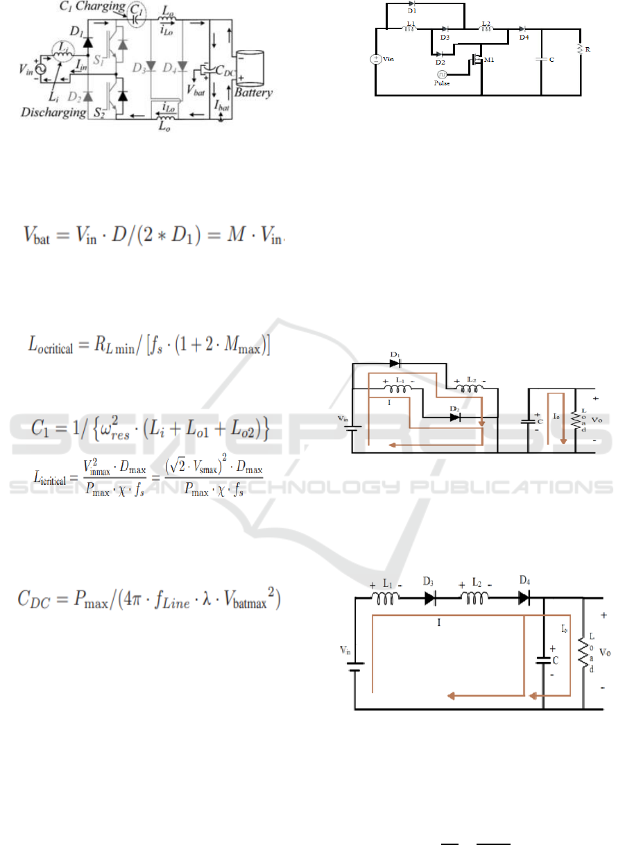
Fig 5: Operation of Mode 3 of BSIC.
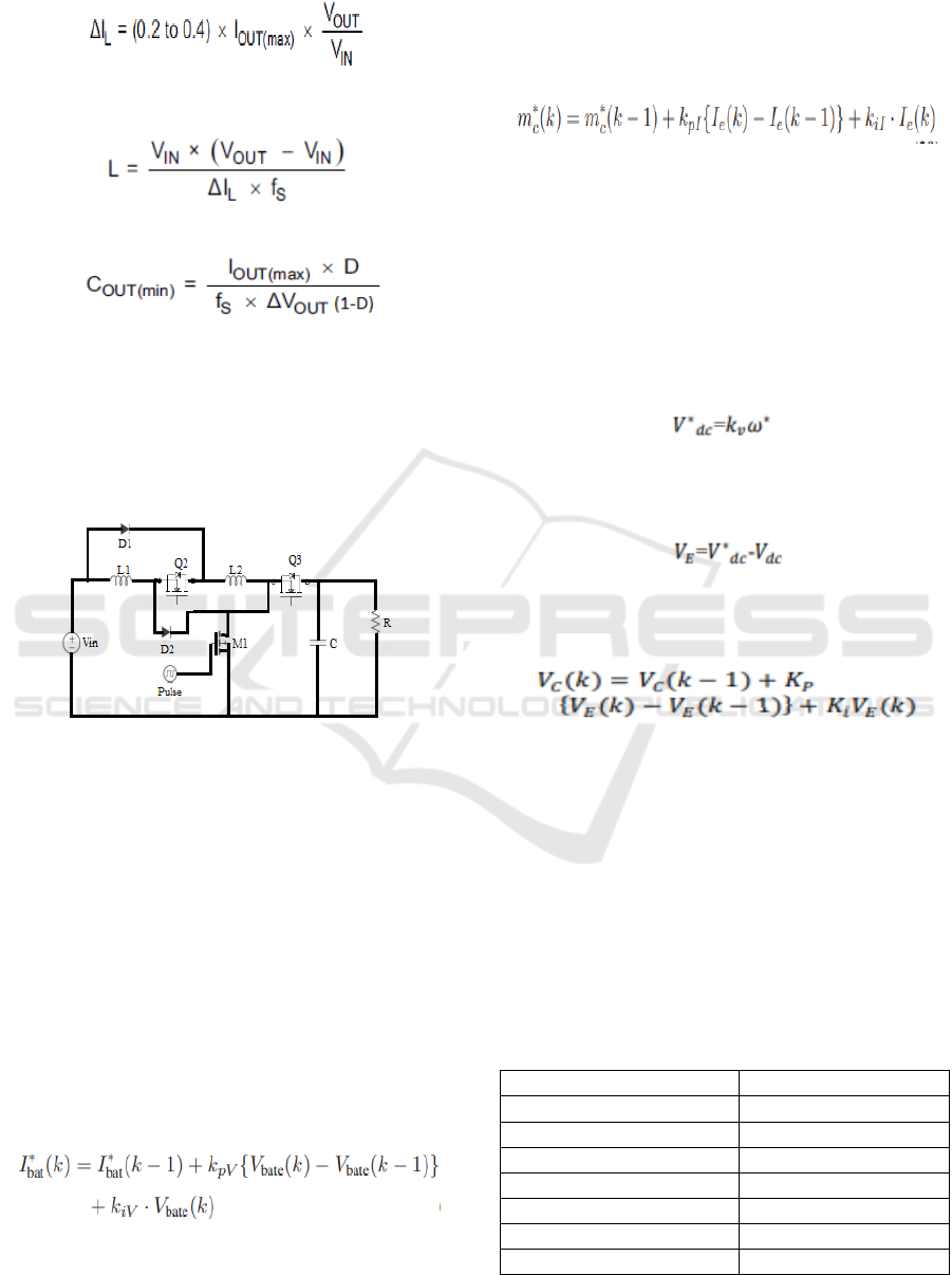
The voltage conversion ratio of the cuk converter is
provided below:
where D1 represents the diodes (D5 and D6) duty
ratio and M= Vbat/Vin.
The load side inductance value is calculated as
provided below:
The source side inductance value is calculated for
CCM is provided below:
The value of C1 is calculated as
where ωres is resonant frequency
CDC is calculated as
where f
line
is the supply frequency.
2.2 High Gain Boost Converter
Similar to a resistor, an inductor behaves as an
appliance and uses energy when it is charged, and
when it is discharged, it acts as a source of energy.
Because the voltage it creates during the phase of
discharge is based on the rate of current change rather
than the starting charging voltage, a variety of
voltages at the input and output are possible. The
following graphic shows the basic layout for a boost
converter with a high voltage conversion ratio:
Fig 6: Basic configuration of high gain boost converter.
The proposed converter operates in one of two
modes while the power electronic switch S is in
operation and in both modes when switch S is turned
off. Inductors L1 and L2 get charged simultaneously
by the source voltage Vin through Diodes D1 and D2,
respectively, when switch S is switched ON. A single
capacitor, four diodes, and a MOSFET switch with a
PWM switching rate make up the power circuit
approach. Capacitor C is discharged by the load. D3
and D4 reverse biased diodes were available. The
operation is depicted in the accompanying figure
while switch S is turned ON.
Fig 7: Operation of converter when switch is ON.
Both inductors are draining while the power
electronic switch S is turned off, and the voltage
source is connected in series by diodes D3 and D4.
D1 and D2 are not conducting at this time.
Fig 8: Operation of converter when switch is OFF.
The design equations for the high gain dc-dc
converter is provided below:
The duty ratio of the high gain converter is
provided below.
𝑉
𝑜
𝑉
𝑖𝑛
=
1 + 𝐷
1 − 𝐷
ISPES 2023 - International Conference on Intelligent and Sustainable Power and Energy Systems
110
The inductor ripple current is provided below
The inductor value is provided by the relation shown
below
The load capacitor value is calculated as follows:
Where ΔVOUT = desired output voltage ripple.
Switches Q2 and Q3 are used in place of the
diodes D2 and D3 for bidirectional power flow; Q3
works at a PWM frequency while Q2 operates at a
lower frequency solely to provide a path for the load
(the battery serves as the load during regenerative
braking).
Fig 9: circuit diagram of converter when diodes are placed
with switches Q1&Q2.
2.3 Control Structure of Basic
Converter
The suggested converter is used to control the
battery's charging current in both CC and CV modes,
depending on the circumstance. While the outer loop
controls variations in Vbat, the inner loop controls
Ibat and maintains UPF operation with the least
amount of distortion. The reference battery current
(Ibat) is obtained by matching the Vbat and Vbat for
the outer loop, and the error (Vbate) is fed into the
proportional-integral (PI) control as an input. The
voltage PI controller's output serves as Ibat. The
specified outer loop expressions are:
where kpV stands for the proportional gain of the
voltage PI controller, kiV for the integral gain, and k
for the sampling moment. Inner loop control is
implemented by comparing the current used to charge
Ibat to Ibat, and sending the error (Ie) to the control
circuit after that.The needed duty ratio (mc) is
provided by the PI controller's output as
where kpI and kiI, respectively, are the gains of the
current PI controller. Next, the duty ratio (mc) is
compared to a carrier waveform. Switch (S1 and S2)
receive the relevant gate drive signals from the
comparison.
2.4 Speed Control Strategy
The DC reference voltage (𝑉
∗
𝑑𝑐
) is provided below is
calculated with the help of reference speed.
The reference voltage (𝑉
∗
𝑑𝑐
) is compared with the
actual load voltage (𝑉
𝑑𝑐
) and the error voltage (𝑉
𝐸
) is
provided below as
The generated error is given to proportional–integral
(PI) control, which provides the reference voltage 𝑉
𝐶
as follows:
The pulses generated for the boost converter is as
follows:
{If 𝑀
𝐶
< 𝑉
𝐶
gating pulse is HIGH}
{If 𝑀
𝐶
≥ 𝑉
𝐶
gating pulse is LOW}
3 SIMULATION SETUP &
RESULTS
The simulation parameters for the proposed
converter are shown below in Table I:
Input Voltage
(160 -230) V
Input power
1500W
Switching Frequency
2 KHZ
Inductor
9.1mH
Coupling Capacitor
55.6µF
Output Capacitor
2mF
Battery voltage
48V
Battery capacity
1.5Ah
Design of a SI Cuk Converter Based on Bridgeless Power Factor Correction with Regenerative Braking
111
DC Motor parameters
150V, 500W, 1500
rpm
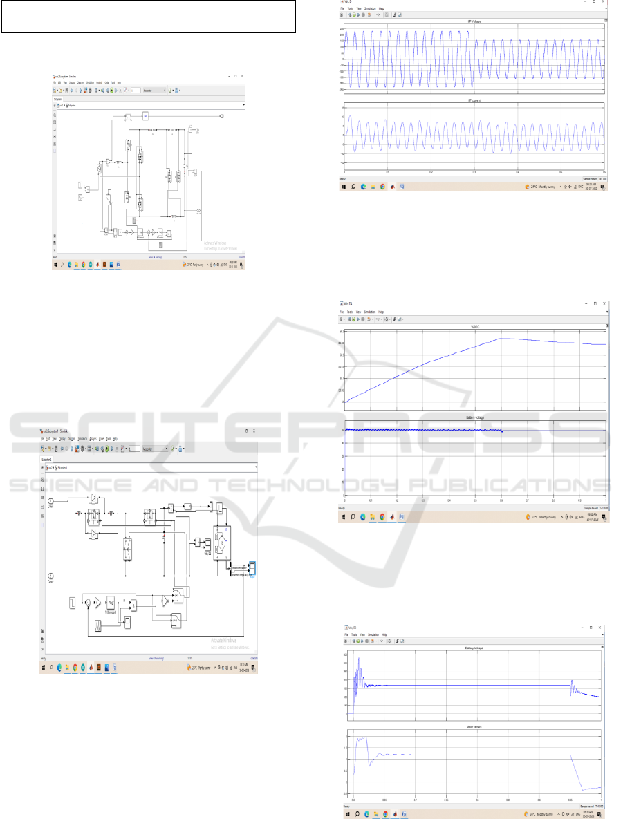
The simulation circuit for the cuk converter with
PI controller is provided below in fig.10.
Figure 10: Simulation circuit.
In this, the supply voltage of 230V is applied to
the proposed converter from t=0 to t=0.3s. Then the
supply changed from 230V to 160V at t=0.3s. During
this two modes, the battery will be charging and the
motor will be in standstill condition. The simulation
circuit for the high gain bidirectional converter with
PI controller is provided below:
Figure 11: Bii-directional converter simulation.
The motor begins to function in the forward
direction and the battery begins to discharge at t=0.6s
(mode 3). Regenerative braking is performed to the
motor at t=0.95s (mode 4), and the charge stored in
the motor windings is extracted to recharge the
battery.
In mode1 and 2, the supply is connected and
charges the battery of the EV. The supply voltage and
current is provided is provided below:
Figure 12: Supply voltage and current.
The supply voltage in this is around 220V and 7A.
The supply charges the battery, and the waveforms of
its voltage and%SOC are shown below
voltage), and the SOC:
This keeps the battery voltage at 52V (which is
greater than the 48V battery nominal percentage is
rising. At t=0.6s, the supply is cut off, and as the
battery begins to discharge and deliver power to the
car, the%SOC starts to fall. Below are the motor
voltage and current values:
Figure 13: Motor voltage and current.
ISPES 2023 - International Conference on Intelligent and Sustainable Power and Energy Systems
112
At t=0.6s, the motor begins to run in the forward
direction with a positive current flow, and at t=0.95s,
regenerative braking is performed with a negative
current flow, or it is supplied back to the battery to
charge it. Below is a list of the battery voltage and
SOC during regenerative braking:
Figure 14: battery voltage and SOC.
The battery is first charged by the source until
t=0.6s, resulting in a high battery voltage and rising
SOC. The soc starts to decrease as the engine turns on
at time t=0.6s as a result of battery discharge.
Regenerative braking is used at time 0.95 seconds,
which recharges the battery once more and raises the
voltage and %SOC.The %THD of the supply current
is provided below:
Figure 15: Total Hamonic Distortion.
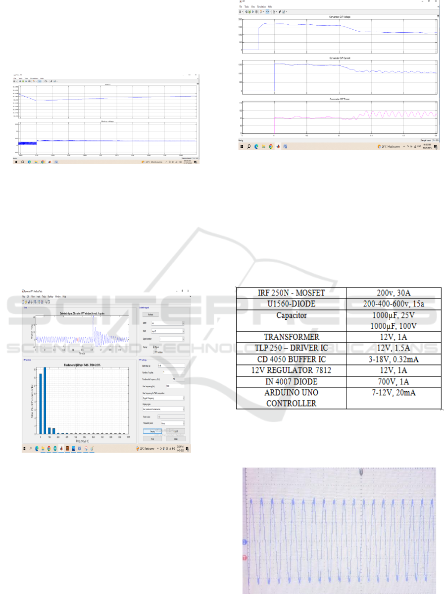
The %THD of the supply current is around 2.01%.
The efficiency of the proposed system is provided
below: With an efficiency of about 95%, the input
power is in the range of 1570W and the output power
is about 1500W.
Figure 16: Simulation results.
Using a battery of 12V, 2.2Ah and a BSIC
converter with an output voltage of 24V, 50 Hz, a
hardware prototype model of the proposed converter
is created. When the battery is being discharged, the
input voltage of the battery is 12V, and the load
voltage of the high gain converter is 48V. The
hardware specifications are listed in Table II below.
Table 2: Hardware Parameters.
The suggested converter uses an Arduino uno
control to generate the pulses, which are then sent to
the driver circuit (TLP 250) to drive the mosfets IRF
250. Below are the input voltage waveforms:
Figure 17: Voltage.
Design of a SI Cuk Converter Based on Bridgeless Power Factor Correction with Regenerative Braking
113
In this the voltage division is 10V/div and the input
voltage is around 24V. It is provided to charge the
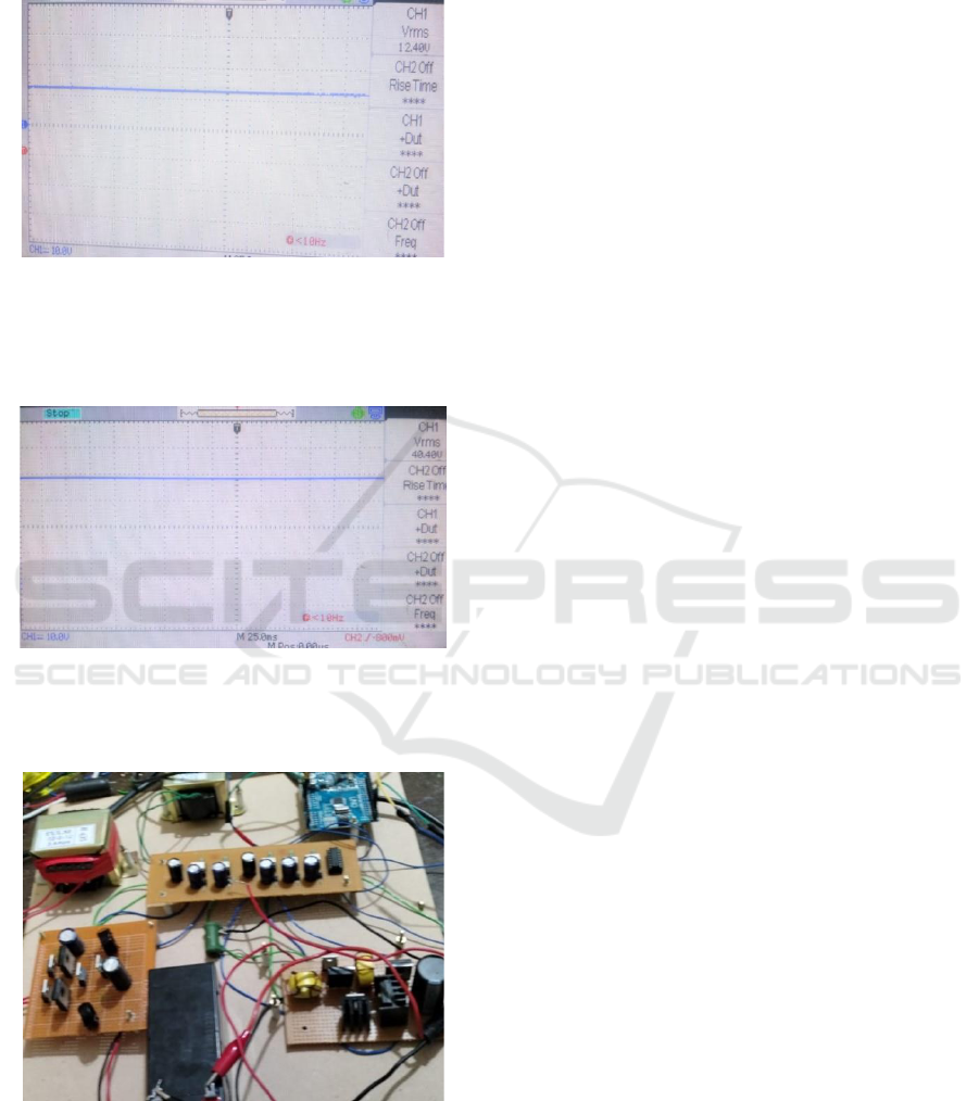
battery. The battery voltage is provided below:
Figure 18: Battery charging and Discharging.
In battery discharging mode, the battery voltage is
provided as input and the load voltage is provided
below:
Figure 19: Load voltage.
The load voltage of the high gain converter is
around 40.4V.
Fig 20: Prototype model of proposed converter.
4 CONCLUSION
The size of the converter is decreased as the bridge is
removed from the switched inductor (SI) based Cuk
converter that was designed in this research for use
with electric vehicles. A high gain bidirectional
converter is introduced to power the motor for the
operation of an electric vehicle after the performance
of the converter under steady state and transient
situations is noted. Regenerative braking is used to
extend the vehicle's range by restoring energy from
the motor to the battery. The simulation results show
that the proposed converter is 95% efficient. A
hardware prototype model was created, and the
suggested system's functionality was checked.
REFERENCES
Lachvajderova, Laura & Kadarova, Jaroslava.
(2021)Analysis Of Internal Combustion Engine
Vehicle, Battery Electric Vehicle And Emissions From
Transport. 21. 21-33.
Wang, L., Qin, Z., Slangen, T., Bauer, P., & van Wijk, T.
(2021). Grid Impact of Electric Vehicle Fast Charging
Stations: Trends, Standards, Issues and Mitigation
Measures - An Overview. IEEE Open Journal of Power
Electronics, 2, 56–74. https://doi.org/10.1109/
ojpel.2021.3054601
Bahrami, Ali. (2020). EV Charging Definitions, Modes,
Levels, Communication Protocols and Applied
Standards. 10.13140/RG.2.2.15844.53123/11
Dulau, Lucian Ioan & Bica, Dorin. (2020). Effects of
Electric Vehicles on Power Networks. Procedia
Manufacturing. 46. 370-377.
10.1016/j.promfg.2020.03.054.
Khalid, Mohd & Khan, Irfan & Hameed, Salman & Asghar,
M. & Ro, Jong-Suk. (2021). A Comprehensive Review
on Structural Topologies, Power Levels, Energy
Storage Systems, and Standards for Electric Vehicle
Charging Stations and Their Impacts on Grid. IEEE
Access. PP. 1-1. 10.1109/ACCESS.2021.3112189.
Das, Manoj & Jain, Sachin. (2021). Review on
Optimization Techniques used for Scheduling of
Electric Vehicle Charging. 1-6.
10.1109/CAPS52117.2021.9730621.
Rachid, A., El Fadil, H., Gaouzi, K., Rachid, K., Lassioui,
A., El Idrissi, Z., & Koundi, M. (2022). Electric Vehicle
Charging Systems: Comprehensive
Review. Energies, 16(1), 255. https://doi.org/10.3390/
en16010255
Habib, S., Khan, M. M., Abbas, F., Sang, L., Shahid, M. U.,
& Tang, H. (2018). A Comprehensive Study of
Implemented International Standards, Technical
Challenges, Impacts and Prospects for Electric
Vehicles. IEEE Access, 6, 13866–13890.
https://doi.org/10.1109/access.2018.2812303
ISPES 2023 - International Conference on Intelligent and Sustainable Power and Energy Systems
114

Sanguesa, J. A., Torres-Sanz, V., Garrido, P., Martinez, F.
J., & Marquez-Barja, J. M. (2021). A Review on
Electric Vehicles: Technologies and Challenges. Smart
Cities, 4(1), 372–404. MDPI. https://doi.org/10.3390/
smartcities4010022
Sanguesa, J. A., Torres-Sanz, V., Garrido, P., Martinez, F.
J., & Marquez-Barja, J. M. (2021). A Review on
Electric Vehicles: Technologies and Challenges. Smart
Cities, 4(1), 372–404. MDPI. https://doi.org/10.3390/
smartcities4010022
Design of a SI Cuk Converter Based on Bridgeless Power Factor Correction with Regenerative Braking
115
