
Assessment of Power Consumption Using a Single Edge Triggering
Flip Flop versus a Clocked CMOS Flip Flop
T. Sindhuja
*
and P. Dass
†
Department of Electronics and Communication Engineering, Saveetha School of Engineering, Saveetha Institute of Medical
and Technical Science, Saveetha University, Chennai, Tamil Nadu, 602105, India
Keywords: Clocked CMOS Flip Flop, Consumption, Flip Flop, MATLAB, Novel Single Edge Triggering Flip Flop,
Power.
Abstract: This study focuses on evaluating the power consumption using a Single Edge Triggering Flip Flop in
comparison with a clocked CMOS Flip Flop. The research is divided into two groups, each consisting of 10
samples: Group 1 involves the design of a clocked CMOS Flip Flop, and Group 2 deals with the design of a
Novel Single Edge Triggering Flip Flop. The sample size was determined using a G power of 80%. Various
length values were employed for the constructed Flip Flops, ranging from 30 nm to 90 nm, utilizing the Gate
Diffusion Input (GDI) technique. The outcomes reveal that the Power Consumption of the Single Edge
Triggering Flip-Flop is 0.5540 watts, whereas the Power Consumption of the clocked CMOS Flip-Flop is
4.7680 watts. The independent sample t-test, with a significance value of p=0.000 (p<0.05), indicates
statistically significant differences in behaviour between the novel Single Edge Triggering Flip Flop and the
clocked CMOS Flip Flop. In conclusion, it is evident that the clocked CMOS Flip Flop consumes more power
than the Single Edge Triggering Flip Flop.
1 INTRODUCTION
CMOS logic circuits hold a significant role across a
wide spectrum of digital applications, spanning from
consumer electronics to industrial control systems.
These circuits constitute a fundamental component in
modern digital design (Thornton 2014). A Flip Flop
featuring a single-edge trigger is a type of digital
electrical circuit designed to store and manipulate
binary data. It is characterized by its triangular shape
and clock input lead. Notably, CMOS devices exhibit
high noise immunity and low static power
consumption, which are their key attributes.
However, due to one of the matched transistors being
always off, the arrangement consumes considerable
energy during transitions between on and off states
(Chang, Dai, and Lin 2023).
Flip Flops find utility in various applications,
including counters, memory units, frequency
dividers, and latches (Sharma et al. 2009). Clocked-
CMOS is a logic family that merges the
synchronization introduced by clock signals with the
*
Research Scholar
†
Project Guide, Corresponding Author
static logic architecture (Lee and Jang 2012). During
its inception, many small-scale integrated (SSI) and
medium-scale integrated (MSI) chips were rooted in
CMOS technology. Even in contemporary design,
this approach remains beneficial for specific
applications, such as dynamic "NORA" circuits
(Mangawati and Palecha 2019).
In recent years, more than 200 articles have been
published, with 89 of them appearing in scientific
journals. Some significant articles in the domain of
low-power Flip Flop design include "Design and
Implementation of Low Power 20 Transistor CMOS
SET Flip Flop" by Kang and Leblebici (2002), "Low
Power Flip Flop Designs Using Different Logic
Styles" by Soudris, Piguet, and Goutis (2002), "A
Revolutionary Low-Power, High-Speed, and
Resilient TSPC Flip-Flop Design" by Pontikakis
(2003), "Low Power Flip Flop Using Double Edge
Triggered Techniques" by Dey et al (2022), and "Low
Power Flip Flop Using Double Edge Triggered
Techniques" by Daroch (2013). These articles
contribute significantly to the field of low-power Flip
Flop design and technology.
508
Sindhuja, T. and Dass, P.
Assessment of Power Consumption Using a Single Edge Triggering Flip Flop versus a Clocked CMOS Flip Flop.
DOI: 10.5220/0012565200003739
Paper published under CC license (CC BY-NC-ND 4.0)
In Proceedings of the 1st International Conference on Artificial Intelligence for Internet of Things: Accelerating Innovation in Industry and Consumer Electronics (AI4IoT 2023), pages 508-513
ISBN: 978-989-758-661-3
Proceedings Copyright © 2024 by SCITEPRESS – Science and Technology Publications, Lda.

In summary, the power consumption comparison
between a 20-transistor CMOS Double Edge
Triggering Flip Flop and a True Single Phase Flip
Flop depends on specific design decisions and usage
scenarios. Different research findings offer
conflicting perspectives, with some suggesting that
the Double Edge Triggering flip-flop consumes less
power than the True Single-Phase Clocking flip-flop,
while others indicate the opposite. In general, it is
evident that the Double Edge Triggering flip-flop
holds promise as a low-power design option that has
the potential to outperform conventional flip-flops in
terms of power efficiency.
Clock CMOS flip-flops are renowned for their
higher power consumption in comparison to other
flip-flop variants. This disparity arises from dynamic
power consumption, stemming from the repetitive
toggling between high and low states within each
clock cycle inherent to clocked CMOS flip-flops. The
consistent charging and discharging of capacitors
within CMOS circuitry contribute to elevated energy
consumption, constituting a limitation for clocked
CMOS flip-flops. The current study aims to assess
power consumption by juxtaposing Single Edge
Triggering Flip Flops against Clocked Flip Flops,
utilizing a 20-transistor model CMOS technology.
2 MATERIALS AND METHODS
The research was carried out within the Department
of Electronics and Communication Engineering at
Saveetha Institute of Medical and Technical Science
(SIMATS), Chennai, specifically at Saveetha School
of Engineering. The investigation involved the testing
of an integrated Flip Flop, with varying lengths
subjected to evaluation. These length measurements
spanned from 30 nm to 90 nm and were assessed
using the Gate Diffusion Input (GDI) technique, as
described in the study titled "Area and Power
Efficient Design of Edge Triggered D Flip Flop Using
GDI Technique" in 2018. The study was divided into
two distinct groups: Group 1 consisted of Clocked
CMOS Flip Flops, while Group 2 featured Novel
Single Edge Triggering Flip Flops. Each group was
composed of a sample size of 10 participants. The
sample size determination was performed using
clincalc.com, incorporating the F Score derived from
prior research studies. In the calculation, the preset
power remained constant at 80%, while the alpha
value was set at 0.05 in accordance with statistical
standards (Brown and Vranesic 2005; Simon 2020).
MATLAB played a pivotal role in this study,
serving as the primary tool for simulations. Its
utilization was crucial for the development and
exploration of engineering projects, products, and
systems. By employing MATLAB, the time required
for product development was significantly reduced,
thereby facilitating strategy validation, control
strategy verification, and the prediction of system
performance (Kumar et al. 2022).
Single Edge Triggering Flip Flop
Single edge triggering flip-flops find extensive use in
digital circuits, primarily due to their ability to
synchronize signals from multiple sources arriving at
different times. These flip-flops effectively mitigate
the risk of data corruption or errors by ensuring that
output updates occur only once per clock cycle. Their
applications span various digital contexts, including
clock domain crossing, data synchronization, and
memory storage. Moreover, they play a crucial role in
sequential logic circuits like counters, shift registers,
and other setups necessitating reliable data storage
and transfer.
Clocked CMOS Flip Flop
In digital systems, clocked CMOS flip-flops play a
pivotal role in holding individual bits of data,
primarily serving timing and synchronization
functions. These flip-flops exhibit notable
advantages, particularly in terms of their simplicity.
Comprising just two cross-coupled inverters, their
design and implementation are relatively
straightforward. Furthermore, their low-power
characteristics render them well-suited for scenarios
demanding minimal power consumption, such as
battery-operated devices or other applications with
stringent power requirements.
Statistical Analysis
SPSS version 26.0, a statistical programming
software, was employed for the analysis of force
estimations in single-edge triggering flip-flop logic
gates when compared to clocked CMOS flip-flop
designs (Bauer 1986). The t-test method was utilized
to generate descriptive insights, encompassing mean,
standard deviation, and standard errors, for each
respective model. This procedure facilitated the
calculation of mean, standard deviation, and standard
error values for the logic gates. In-depth analysis was
conducted using an independent samples t-test,
involving both the dependent and independent
variables. The study outlined that the independent
variables correspond to single-edge flip-flops, while
the dependent variable pertains to power.
Assessment of Power Consumption Using a Single Edge Triggering Flip Flop versus a Clocked CMOS Flip Flop
509

Table 1: The power value of Clocked CMOS Flip Flop and Single Edge Triggering Flip Flop.
S.NO
Group 1
Power Clocked CMOS Flip Flop
Group 2
Power Single Edge
Triggering Flip Flop
1
4.98
0.50
2
4.92
0.51
3
4.88
0.53
4
4.83
0.54
5
4.77
0.54
6
4.71
0.56
7
4.68
0.58
8
4.66
0.59
9
4.62
0.59
10
4.62
0.60
Table 2: This table compares the single-edge triggering Flip Flop and Clocked CMOS Flip Flop, here the Clocked CMOS
Flip Flop (4.7680) has the higher mean value when compared to the single-edge triggering Flip Flop (.5540).
Group
No.of
Samples
Mean
Std.
deviation
Std. mean
error
Power
Clocked
CMOS Flip
Flop
10
4.7680
.12831
.04057
Novel Single
Edge
Triggering
Flip Flop
10
.5540
.03534
.01118
3 RESULTS
Table 1 displays the power values obtained from the
comparison between Single Edge Triggering Flip
Flop and clocked CMOS Flip Flop, considering a
sample size of 10.
Table 2 presents the mean, standard deviation, and
standard errors of Power Consumption for Clocked
CMOS Flip Flop and Single Edge Triggering Flip
Flop, respectively.
Table 3 showcases that a clocked CMOS flip flop
consumes 4.7680 watts of power, while a Single Edge
Triggering Flip Flop utilizes only 0.5540 watts. The
results highlight a statistically significant distinction
between the innovative Single Edge Triggering Flip
Flop and the double edge triggering Flip Flop
(p=0.000), as determined by an independent sample
t-test (p < 0.05).
Figure 1 illustrates the circuit diagram designed to
detect Single Edge Triggering Flip Flops.
Figure 2 depicts the output waveform generated
by a Single Edge Triggering Flip Flop.
Figure 3 provides a graphical representation
comparing the power consumption of Single Edge
Triggering Flip Flop and clocked CMOS Flip Flop.
This graph compares the mean power values and
assists in determining the more efficient power
consumption.
AI4IoT 2023 - First International Conference on Artificial Intelligence for Internet of things (AI4IOT): Accelerating Innovation in Industry
and Consumer Electronics
510
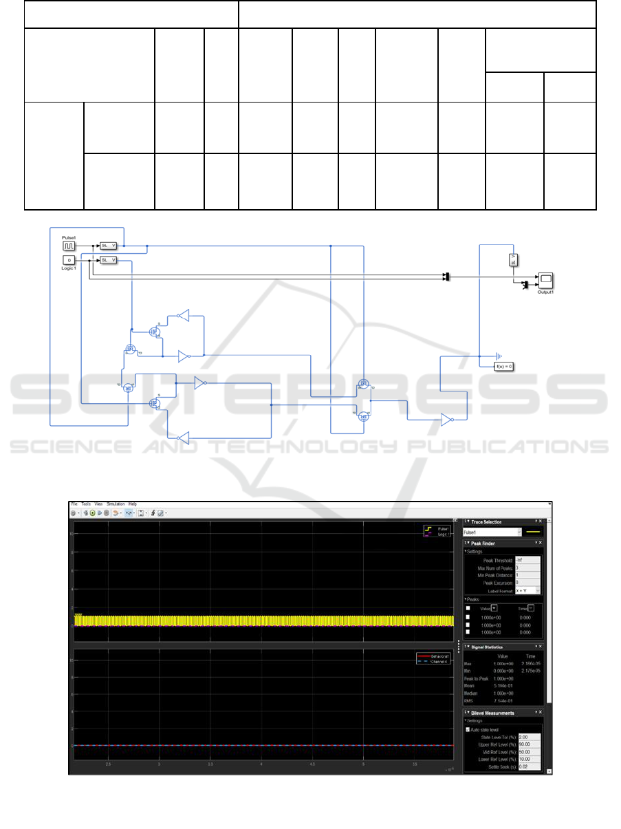
Table 3: The Independent Sample T Test is performed. It demonstrates a statistical difference with p=.000 between the
innovative Single Edge Triggering Flip Flop and the double edge triggering Flip Flop (independent sample t-test p < 0.05).
Levene's test for equality of variances
T-test for equality of means
F
Sig
t
df
Sig
(2-
tailed)
Mean
difference
Std.
error diff
95% confidence
interval of the
difference
lower
upper
POWER
Equal
variances
assumed
16.219
.001
100.132
18
.000
4.21400
.04208
4.12558
4.30242
Equal
variances not
assumed
100.132
10.358
.000
4.21400
.04208
4.12067
4.30733
Figure 1: The schematic picture of a Flip Flop design in which only one transistor is timed by a brief pulse train, which is
known as a Single Edge Triggering Flip-Flop, is used to monitor power consumption using the MATLAB programme.
Figure 2: A novel Single Edge Triggering Flip Flop's output waveform. The output calculates the delay time and the total
energy used.
Assessment of Power Consumption Using a Single Edge Triggering Flip Flop versus a Clocked CMOS Flip Flop
511
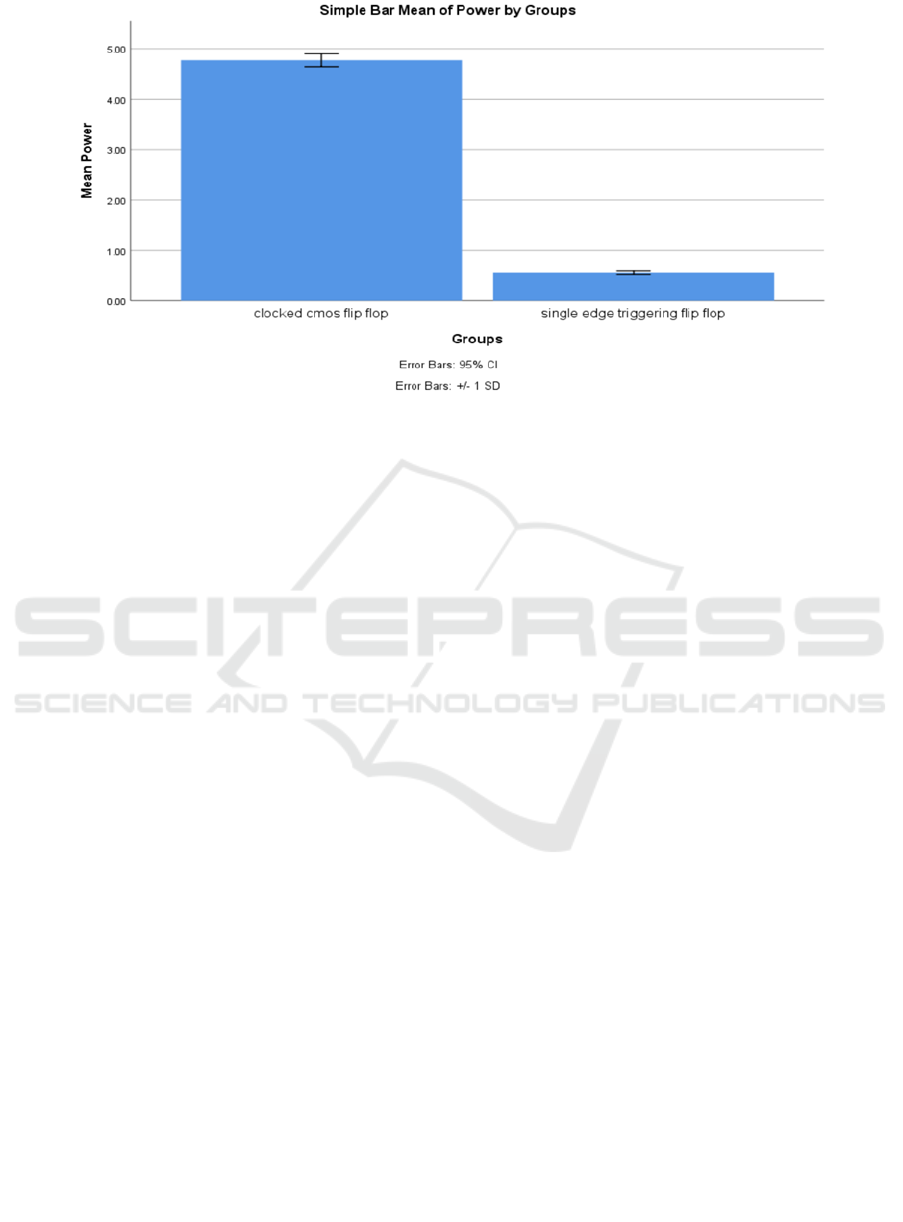
Figure 3: The bar graph shows the variation in the mean power in which it represents Clocked CMOS flip-flop and single-
edge triggering flip-flop with a standard deviation of +/-1SD. The x-axis represents the groups and the y-axis represents the
mean power. It can be seen that a single-edge triggering flip-flop consumes less power compared to a Clocked CMOS flip-
flop.
4 DISCUSSIONS
The method involves analysing the Power
Consumption of a single-edge flip-flop while varying
the logic gates. It was observed that the obtained
value is statistically significant with a p-value of
p=.000. Transistors are utilized at both the latch stage
and the input of the comparison preamplifier. A single
local clock generator manages both phases of
operation. The D FlipFlop can be understood through
the use of a delay line or zero-order hold. The D input
signal is captured as soon as the flip-flop is clocked,
and any subsequent changes to the D input are
delayed until the following clock event. This gives the
D flip-flop an advantage over the D-type transparent
latch in this aspect (Wenckebach and Cox 2023).
Single-edge triggering Flip Flops offer several
advantages compared to Clocked CMOS Flip Flops.
Firstly, they require fewer transistors and are less
complex in their design. Secondly, single-edge
triggering Flip Flops operate on only one clock edge,
leading to a reduction in the number of clock signal
transitions and subsequently lowering Power
Consumption. Additionally, it's possible to design
single-edge triggering Flip Flops with reduced
voltage swings, contributing to lower power
consumption overall (Noh et al. 2012).
However, single-edge triggering Flip Flops are
vulnerable to glitches, which are unwanted pulses
caused by circuit disturbances or noise. These
glitches can lead to incorrect data being stored in the
flip-flop. For the future, designers can explore
techniques like glitch filtering, signal conditioning,
and clock gating to mitigate the impact of glitches on
the input data signal and reduce the likelihood of
incorrect data being stored in the flip-flop.
5 CONCLUSION
The study results indicate that Single Edge Triggering
Flip Flops consume 0.5540 watts of power, whereas
Clocked CMOS Flip Flops consume 4.7680 watts of
power. This suggests that Single Edge Triggering Flip
Flops exhibit lower Power Consumption compared to
Clocked CMOS Flip Flops.
REFERENCES
Brown, Stephen D., and Zvonko G. Vranesic. (2005).
Fundamentals of Digital Logic with VHDL Design.
Chang, Chun-Rong, Zih-Jyun Dai, and Chun-Yu Lin.
(2023). “π-Shape ESD Protection Design for Multi-
Gbps High-Speed Circuits in CMOS Technology.”
Materials 16 (7). https://doi.org/10.3390/ma16072562.
Daroch, Rohit. (2013). Double Edge Triggered Flip Flop.
Dey, N., Kumar, G., Vickram, A. S., Mohan, M., Singhania,
R. R., Patel, A. K., ... & Ponnusamy, V. K. (2022).
Nanotechnology-assisted production of value-added
biopotent energy-yielding products from
AI4IoT 2023 - First International Conference on Artificial Intelligence for Internet of things (AI4IOT): Accelerating Innovation in Industry
and Consumer Electronics
512

lignocellulosic biomass refinery–a review. Bioresource
technology, 344, 126171.
George, Darren, and Paul Mallery. (2019). IBM SPSS
Statistics 26 Step by Step: A Simple Guide and
Reference. Routledge.
Joseph, Jean B., Paulo Marcelo V. Ribeiro, Leonardo J. N.
Guimarães, Cicero Vitor Chaves Junior, and Jonathan
D. A. C. Teixeira. (2022). “Acceleration Strategies for
Tridimensional Coupled Hydromechanical Problems
Based on CPU and GPU Programming in MATLAB.”
Anais Da Academia Brasileira de Ciencias 94 (suppl
4): e20211024.
Kang, Sung-Mo, and Yusuf Leblebici. (2002). CMOS
Digital Integrated Circuits: Analysis and Design.
Kumari, Sweta, V. Y. Shobha Amala, M. Nivethithan, and
V. Srinivasa Chakravarthy. (2022). “BIAS-3D: Brain
Inspired Attentional Search Model Fashioned after
What and Where/how Pathways for Target Search in
3D Environment.” Frontiers in Computational
Neuroscience 16 (November): 1012559.
Lee, Han-Yeol, and Young-Chan Jang. (2012). “A True
Single-Phase Clocked Flip-Flop with Leakage Current
Compensation.” IEICE Electronics Express.
https://doi.org/10.1587/elex.9.1807.
Li, He, Yimeng Zhang, and Tsutomu Yoshihara. (2013).
“Clocked CMOS Adiabatic Logic with Low-Power
Dissipation.” 2013 International SoC Design
Conference (ISOCC).
https://doi.org/10.1109/isocc.2013.6863986.
Lin, Jin-Fa, Zheng-Jie Hong, Chang-Ming Tsai, Bo-Cheng
Wu, and Shao-Wei Yu. (2020) “Novel Low-
Complexity and Low-Power Flip-Flop Design.”
Electronics.
https://doi.org/10.3390/electronics9050783.
Lyne, Christopher T., Miron F. Liu, and Joshua L. Rovey.
(2023). “A Simple Retarding-Potential Time-of-Flight
Mass Spectrometer for Electrospray Propulsion
Diagnostics.” Journal of Electric Propulsion 2 (1): 13.
Mangawati, Akshay S., and Namita Palecha. (2019).
“Clock Gating Integration Using 18T-TSPC Clocked
Flip Flop.” 2019 2nd International Conference on
Intelligent Computing, Instrumentation and Control
Technologies (ICICICT).
https://doi.org/10.1109/icicict46008.2019.8993329.
Noh, Jinsoo, Minhun Jung, Kyunghwan Jung, Gwangyong
Lee, Soyeon Lim, Daae Kim, Vivek Subramanian, and
Gyoujin Cho. (2012). “All Printed Edge-Triggered
Register Using Single Walled Carbon Nanotube-Based
Thin Film Transistor.” Journal of Nanoscience and
Nanotechnology 12 (5): 4261–64.
Pontikakis, Bill. (2003). A Novel Double Edge-Triggered
Pulse-Clocked TSPC D Flip-Flop for High-
Performance and Low-Power VLSI Design
Applications.
Ramalakshmi, M., & Vidhyalakshmi, S. (2021). GRS
bridge abutments under cyclic lateral push. Materials
Today: Proceedings, 43, 1089-1092.
Ramkumar, G. et al. (2022). “Optimization of Solar Hybrid
Power Generation Using Conductance-Fuzzy Dual-
Mode Control Method” International Journal of
Photoenergy, Volume 2022, Article ID 7756261, 10
Pages, 2022 https://doi.org/10.1155/2022/7756261
Sharma, Manoj, Arti Noor, Satish Chandra Tiwari, and
Kunwar Singh. (2009). “An Area and Power Efficient
Design of Single Edge Triggered D- Flip Flop.” 2009
International Conference on Advances in Recent
Technologies in Communication and Computing.
https://doi.org/10.1109/artcom.2009.207.
Simon, Francesca. (2020). Horrid Henry 2020 Summer
Bind-Up. Orion Children’s Books.
Soudris, Dimitrios, Christian Piguet, and Costas Goutis.
(2002). Designing CMOS Circuits for Low Power.
Taylor & Francis US.
S. K. Sarangi, Pallamravi, N. R. Das, N. B. Madhavi, P.
Naveen, and A. T. A. K. Kumar, “Disease Prediction
Using Novel Deep Learning Mechanisms,” J. Pharm.
Negat. Results, vol. 13, no. 9, pp. 4267–4275, 2022, doi:
10.47750/pnr.2022.13.S09.530
Thornton, Mitchell A. (2014). “Modeling Digital Switching
Circuits with Linear Algebra.” Synthesis Lectures on
Digital Circuits and Systems.
https://doi.org/10.2200/s00579ed1v01y201404dcs044.
V. P. Parandhaman, (2023)"A Secured Mobile Payment
Transaction Handling System using Internet of Things
with Novel Cipher Policies," International Conference
on Advances in Computing, Communication and
Applied Informatics (ACCAI), Chennai, India, 2023,
pp. 1-8, doi: 10.1109/ACCAI58221.2023.10200255.
Wenckebach, W. Th, and S. F. J. Cox. (2023). “Nuclear
Dipolar Relaxation Induced by Interacting Ground
State Electron Spins.” Journal of Magnetic Resonance
348 (March): 107375.
Assessment of Power Consumption Using a Single Edge Triggering Flip Flop versus a Clocked CMOS Flip Flop
513
