
High-Speed Pipelined FPGA Implementation of a Robust
Steganographic Scheme for Secure Data Communication Systems
Salah Harb
a
, M. Omair Ahmad
b
and M. N. S. Swamy
c
Electrical and Computer Engineering Department, Concordia University, 1440 De maisonnueve, Montreal, Canada
Keywords:
Information Hiding, Steganography, Communication Systems, FPGA, Pipelined Architecture, Efficiency.
Abstract:
In this paper, we introduce a high-speed and area-efficient hardware design for a novel modulus-based image
steganographic scheme, specifically targeting constrained-area steganographic embedded systems. The pro-
posed modulus-based image steganography scheme enhances both image quality and embedding rate while en-
suring resilience against PVD histogram analysis, salt-and-pepper noise, and RS analysis attack. The hardware
architecture incorporates pipelined registers placed to guarantee balanced-execution paths among computing
components. A memory-less finite state machine model is developed to efficiently control the instructions for
the steganographic operations. Employing a hardware-software co-design approach, the proposed hardware
design is realized as an IP core on the AMD Xilinx Zynq-7000 APSoC platform. It processes concealing
operations in just 13 clock cycles, utilizes 148 slices, and operates at 290 MHz. This results in a remarkable
throughput of 2.32 Gbps. The hardware design demonstrates significant improvements in speed, resource
utilization, and throughput compared to recent steganographic hardware implementations, making it ideal for
resource-constrained, real-time applications ranging from secure embedded communication to advanced IoT
data protection.
1 INTRODUCTION
In the realm of digital secure data communication, the
art of information hiding has become increasingly sig-
nificant. As digital communication proliferates, en-
abling the easy distribution of assets like images and
videos, it simultaneously raises critical security con-
cerns. Information hiding techniques are pivotal in
addressing these concerns, as they encompass meth-
ods for both embedding secret data in digital carriers
(steganography) and transforming it (cryptography).
Among these techniques, image steganography
plays a crucial role. It ensures the covert transmis-
sion of confidential data within an image. The core
components of this process involve a cover image and
a steganographic scheme. The primary function of
the steganographic scheme is to conceal secret data
within the cover image, creating what is known as a
stego image. This process of concealing secret data
into the cover image is referred to as the embedding
process. Conversely, the process of retrieving the hid-
a
https://orcid.org/0000-0002-5975-6537
b
https://orcid.org/0000-0002-2924-6659
c
https://orcid.org/0000-0002-3989-5476
den data from the stego image is called the extracting
process. To an unsuspecting receiver, the stego im-
age appears ordinary, yet it carries hidden information
that can only be extracted by the intended receiver us-
ing a shared key. Figure 1 illustrates the main compo-
nents of the image steganography process.
Embedding
process
Sender
Cover
image
Exraction
process
Receiver
Shared
private key
Stego
image
Cover
image
Secret data Secret data
Figure 1: Main components of the image steganography.
Image steganography for data transmission oper-
ates either in frequency domain for enhanced secu-
rity (Kumar and Kumar, 2018; Fakhredanesh et al.,
2019; Sukumar et al., 2021; Mandal et al., 2022)
or spatial domain, which alter pixels directly. The
latter includes interpolation-based (Lu, 2018; Shaik
and V, 2019; Hassan and Gutub, 2021), encryption-
based (Zhang et al., 2016; Zhang et al., 2019; Wu
et al., 2021), and modulus-based schemes (Zhang and
Wang, 2006; Chao et al., 2009; Kuo et al., 2016; Liu
et al., 2019; Saha et al., 2020; Kumar and Jung, 2020;
Leng et al., 2021). Modulus-based schemes are fa-
Harb, S., Ahmad, M. and Swamy, M.
High-Speed Pipelined FPGA Implementation of a Robust Steganographic Scheme for Secure Data Communication Systems.
DOI: 10.5220/0012716700003767
Paper published under CC license (CC BY-NC-ND 4.0)
In Proceedings of the 21st International Conference on Security and Cryptography (SECRYPT 2024), pages 397-406
ISBN: 978-989-758-709-2; ISSN: 2184-7711
Proceedings Copyright © 2024 by SCITEPRESS – Science and Technology Publications, Lda.
397

vored for their balance of image quality, embedding
capacity, and resistance to attacks.
The implementation of image steganography can
be executed on either software or hardware platforms.
While software offers versatility, it often lacks the
speed required for high-performance tasks, leading
to a shift towards hardware solutions for better effi-
ciency. Traditional CPUs and ASICs, although fast,
face design constraints and high costs respectively.
FPGA platforms, such as the AMD Xilinx Zynq-7000
APSoC introduced in 2011, provide a good balance
with their ability to handle complex steganographic
schemes efficiently due to their parallel processing ca-
pabilities, combining hardware efficiency with soft-
ware flexibility.
This paper presents a novel approach to im-
age steganography, implementing a modulus-based
steganographic scheme optimized for the AMD Xil-
inx Zynq-7000 APSoC platform. The proposed
scheme conceals large volumes of secret data within
small pixel groups, thus enhancing image quality
without compromising security. The hardware de-
sign, developed and implemented using the AMD Xil-
inx Vivado 2022.1 suite, adopts a hardware-software
co-design approach. This ensures high-throughput
processing through optimal pipelining stages.
The rest of the paper is organized as follows.
Section 2 provides a comprehensive overview of
modulus-based steganographic schemes. Section
3 introduces a novel modulus-based steganographic
scheme. Section 4 describes the proposed hardware
architecture for the proposed image steganographic
scheme. Finally, Section 5 concludes the paper.
2 MODULUS-BASED
STEGANOGRAPHIC SCHEMES
Modulus-based steganographic schemes, exploiting
modification direction (EMD) (Zhang and Wang,
2006) and diamond encoding (DE) (Chao et al.,
2009), ensure comparable or better stego image qual-
ity with reduced computational complexity than their
interpolation and encryption-based peers. This sec-
tion provides a brief introduction to these two foun-
dational schemes.
2.1 EMD and DE Schemes
In 2006, Zhang and Wang introduced a stegano-
graphic scheme that adopts a data hiding method us-
ing a (2m + 1)-ary notational system. The method
conceals secret data within m consecutive pixels, with
only one pixel in the group being adjusted either by
incrementing, decrementing, or maintaining its orig-
inal value. The embedding process in the EMD
method starts by calculating the value of the weighted
sum modulo function given by
F
EMD
=
m
∑
i=1
(i g
i
) mod (2m +1) (1)
where g
i
denotes the value of the ith pixel. The
difference between the secret data and F
EMD
directs
the pixel modification as follows. (i) if s = 0, no pix-
els are modified, (ii) if s ≤ m, the pixel value g
s
is
incremented by 1, and (iii) if s > m, the pixel value
g
2m+1−s
is decremented by 1.
Figure 2 shows all the possible modifications in
the pixel values in a group of two pixels (m = 2). The
concealed digit E is extracted from the modified pixel
group using the weighted sum modulo function, de-
fined as
g
1
, g
2
,g
3
g
1
, g
2
+1,g
3
g
1
+1, g
2
,g
3
g
1
, g
2
,g
3
+1
g
1
, g
2
-1,g
3
g
1
-1, g
2
,g
3
g
1
, g
2
,g
3
-1
p +1, q
p
, q
p ,q
+1
p -1, q
p ,q
-1
p +2, q
p -2, q
p -1, q
+1
p -1, q
-1
p , q
-2
p , q
+2
p +1, q
-1
p +1, q
+1
Figure 2: All possible modifications for pixels when m = 2.
E = F
EXT EMD
=
m
∑
i=1
i · g
′
i
mod (2m + 1) (2)
In order to improve the embedding capacity pro-
vided by the EMD, a steganographic scheme employ-
ing diamond encoding (DE) method was introduced
by (Chao et al., 2009). Within this DE method, a
concealed digit E, expressed in the (2k
2
+2k +1)-ary
notational system, is concealed into only two pixels
p, q of in the cover image. Unlike the EMD scheme,
this scheme allows modifications to either one or both
pixel values, adjusting them within the range [−k,k]
or leaving them intact. The embedding process in the
DE method starts by calculating the value of the mod-
ulo function defined by
F
DE
= ((2k + 1)p + q) mod (2k
2
+ 2k + 1) (3)
It should be noted that F
DE
falls within the range
[0,2k
2
+ 2k]. To determine which change from the
various possible modifications in the diamond of S
k
should be applied to (p,q), the modulus distance d
k
between the values of the secret digit E and F
DE
is
calculated using:
d
k
= (E −F
DE
) mod (2k
2
+ 2k + 1) (4)
The modulus distance d
k
will be in the range
[0,2k
2
+ 2k]. The set of values for d
k
, denoted by D
k
,
SECRYPT 2024 - 21st International Conference on Security and Cryptography
398

can also be arranged in a diamond shape pattern. In
this pattern, each d
k
value corresponds to a vector in
S
k
, which provides the new values for (p,q). Figure 3
illustrate the distance patterns for D
2
.
The secret digit E can be extracted from the mod-
ified values (p
′
,q
′
) of the stego image by utilizing the
modulo function:
E = F
EXT DE
= ((2k+1)p
′
+q
′
) mod (2k
2
+2k +1)
(5)
g
1
, g
2
,g
3
g
1
, g
2
+1,g
3
g
1
+1, g
2
,g
3
g
1
, g
2
,g
3
+1
g
1
, g
2
-1,g
3
g
1
-1, g
2
,g
3
g
1
, g
2
,g
3
-1
p +1, q
p
, q
p ,q
+1
p -1, q
p ,q
-1
p +2, q
p -2, q
p -1, q
+1
p -1, q
-1
p , q
-2
p , q
+2
p +1, q
-1
p +1, q
+1
Figure 3: All possible modifications for pixels when k = 2.
In the EMD scheme, the choice of m is pivotal for
balancing the embedding rate and image quality, as
noted in (Zhang and Wang, 2006). At m = 2, EMD
achieves its peak embedding rate of 1.16bpp. Larger
m values enhance stego image quality but decrease
the rate. Conversely, the DE scheme is optimal in im-
age quality at k = 1. Using the Lena cover image at a
100% payload yields a PSNR of 52.1dB and an em-
bedding rate of 1.16 bpp. Increasing k raises the rate
but diminishes stego image quality.
3 PROPOSED MODULUS-BASED
STEGANOGRAPHIC SCHEME
For a given secret data block size, L, the EMD scheme
provides a stego image with a specific image quality
and embedding rate. Similarly, the DE scheme pro-
vides a stego image with its own image quality and
embedding rate. When L decreases, the EMD scheme
delivers a decline in image quality and an uptick in
embedding rate. Conversely, with the DE scheme,
the trend is the opposite, as L decreases, image qual-
ity improves while the embedding rate drops. This
behavior is also observed when L increases; how-
ever, the roles reverse, the EMD scheme results in
enhanced image quality and reduced embedding rate,
while the DE scheme experiences decreased image
quality and a boosted embedding rate.
Given the above observations, it is essential to
consider a steganographic scheme that ensures a bal-
ance performance regardless of the secret data block
size L. Ideally, such a scheme would surpass the max-
imum embedding rate of the DE scheme while of-
fering superior image quality compared to the EMD
scheme. One approach could involve segmenting
each L-sized secret data block into L
1
and L
2
, embed-
ding them using EMD and DE schemes, respectively.
By doing so, we achieve a balance in image quality
and embedding rate superior to solely using the EMD
or DE scheme.
To further enhance the image quality and embed-
ding rate, two lookup tables are constructed, repre-
senting the two segments L
1
and L
2
. The segment L
1
is searched within the first lookup table to retrieve two
secret digits, S
0
and S
1
, which represent L
1
. Similarly,
the segment L
2
is located within the second lookup ta-
ble to obtain the secret digit S
2
that represents L
2
.
3.1 The Algorithm
A secret data block B of size L is divided into two
segments of sizes L
1
and L
2
. The first segment is rep-
resented by two secret digits, which are concealed by
the EMD scheme using the (2n + 1)-ary notational
system. The second segment is represented by one
secret digit, and this is concealed by the DE scheme
using the (2k
2
+ 2k + 1)-ary notational system.
Figure 4 depicts the first lookup table for L
1
= 4
bits with m
x
= 2 and m
y
= 2. Given that L
1
= 4
bits, the table comprises 16 (2
4
) entries. The val-
ues for these entries span the range [0,2
4
− 1] or
[0000,1111]
2
. Each value in this table corresponds
to the first segment L
1
of the secret data block with
size L . The table is aligned along the x - and y-
coordinate axes, with each axis using its own nota-
tional system to denote secret digits. In particular, the
x-coordinate axis encapsulates all 2m
x
possible values
from the (2m
x
+1)-ary system, while the y-coordinate
axis encompasses all 2m
y
possible values from the
(2m
y
+ 1)-ary system. As illustrated in Figure 4, the
x-coordinate axis ranges from [0, 4] for a group of 2
pixels, and similarly, the y-coordinate axis also spans
[0, 4] for a group of 2 pixels.
0
0
1 2 3 4
1
2
3
4
xx xx xx xx xx
15 xx xx xx xx
10 11 12 13 14
5 6 7 8 9
0 1 2 3 4
xx xx xx xx xx
15 xx xx xx xx
10 11 12 13 14
5 6 7 8 9
0 1 2 3 4
2m
x
2m
y
Figure 4: The x − y-coordinate lookup table when L
1
= 4.
After constructing the x −y coordinate lookup ta-
ble, the coordinates (x,y) are determined by searching
for the value of L
1
. The values of these coordinates,
High-Speed Pipelined FPGA Implementation of a Robust Steganographic Scheme for Secure Data Communication Systems
399

(x,y), denote secret digits S
0
and S
1
. Here, S
0
corre-
sponds to the x-coordinate and S
1
to the y-coordinate,
both representing the value of L
1
. These secret dig-
its are then embedded in two groups of pixels, Q
0
and Q
1
, using the EMD scheme. Specifically, the Q
0
group uses m
x
pixels to embed the secret digit S
0
, and
the Q
1
group uses m
y
pixels to embed S
1
.
For the segment L
2
, an additional z-coordinate
axis is introduced to conceal a third secret digit, S
2
,
which represents L
2
using the DE scheme. The z-
coordinate axis uses the vector set S
m
z
within the
(2m
2
z
+ 2m
z
+ 1)-ary notational system. By searching
for L
2
in the distance pattern D
m
z
, one can determine
the specific vector s
m
z
to be concealed within the third
group Q
2
of two pixels, denoted as (p,q). Figure 5 il-
lustrates the z coordinate lookup table when L
2
= 3.
For this segment, the suitable value for the m
z
= 2. It
can be seen from this figure that the z-coordinate axis
also represents the DE distance pattern D
2
.
(+1, 0)
(0, 0)
(0, +1)
(-1, 0)
(0, -1)
(+2, 0)
(-2, 0)
(-1, +1)
(-1, -1)
(0, -2)
(0, +2)
(+1, -1)
(+1, +1)
+ m
z
- m
z
- m
z
+ m
z
50
1
8
12
103
9
7
11
2
4
6
Figure 5: The z-coordinate lookup table when L
2
= 3.
The three secret digits S
0
, S
1
and S
2
, represent the
secret data block B of size L, and three groups of pix-
els Q
0
, Q
1
and Q
2
, are utilized to conceal them, re-
spectively. The entire concealing process is summa-
rized in Algorithm 1.
In the EMD scheme, the secret data block of size
L can be represented using ⌈
L
log
2
(2m+1)
⌉ (2m +1)-ary
secret digits. For example, if L = 7, then m = 6 and
the number of secret digits required is ⌈
7
log
2
(2m+1)
⌉
or 2 of 13-ary secret digits to represent a 7-bit secret
data block. Each secret digit is concealed into a 6-
pixel group, thus, 2 of 13-ary secret digits need 12
pixels to conceal the secret data block of 7-bit size. In
the DE scheme, the secret data block of size L can be
represented using a distance pattern D
k
that contains
(2k
2
+ 2k + 1) secret digits. For example, if L = 8,
then k = 11 and D
11
has 265 secret digits.
On the other hand, using the proposed scheme, if
the size of the secret data block L = 7 and the pa-
rameters for the x − y − z coordinate lookup table are
m
x
= 2, m
y
= 2, m
z
= 2, L
1
= 4, and L
2
= 3, then the
x-axis for the x −y coordinate lookup table is 2m
x
and
it requires 2 pixels, and the y-axis in the table is 2m
y
Algorithm 1: Proposed modulus-based image stegano-
graphic scheme.
Input: Cover image, segments (L
1
,L
2
), a
stream of L-bit secret data blocks B
Output: Stego image
1 Initialization: x − y coordinate lookup table
(0 : 2m
x
,0 : 2m
y
) with entries:
[0 : 2
C
EMD
− 1] and x − y − z coordinate
lookup table (−m
z
: +m
z
,−m
z
: +m
z
) with
entries: [0 : 2m
2
z
+ 2m
z
]
2 while Num(B) ̸= 0 do
3 Q
0
= m
x
-pixels,Q
1
= m
y
-pixels,Q
2
=
(p,q);
4 (x,y) ← x-y Lookup table(L
1
);
5 D
m
z
← z Lookup table(L
2
);
6 S
0
← x,S
1
← y,S
2
← D
m
z
;
7 EMD[S
0
] using Q
0
group (2m
x
+
1)-ary system;
8 EMD[S
1
] using Q
1
group (2m
y
+
1)-ary system;
9 DE[S
2
] using Q
2
group with (2m
2
z
+
2m
z
+ 1)-ary system;
and it requires 2 pixels. Also, 2 pixels are required
for the L
2
with k = 2 and D
2
has 13 secret digits. This
indicates that our scheme requires a total of 6 pixels
to conceal the L = 7, which is fewer pixels than the
EMD scheme and has smaller distance patterns than
the DE scheme.
The proposed scheme offers a simplified approach
to the conversion of secret data blocks into l-ary dig-
its. The conversion process is avoided, which elimi-
nates the need for complex operations like multiplica-
tion and division, especially when the cut-offs L
1
and
L
2
are large. Instead, the secret data blocks are stored
directly in the lookup tables, and the secret digits S
0
,
S
1
, and S
2
are used for concealing. This approach
provides an additional layer of security since the se-
cret data are not directly involved in the concealing
process.
The complexity of the proposed scheme is primar-
ily limited to the construction of the lookup table. The
construction process becomes more complex as the
size of L increases and the cut-off lengths L
1
and L
2
are increased. Larger cut-off values lead to more en-
tries in the lookup tables, resulting in a more com-
plex construction process. However, this process only
needs to occur once at the beginning of the communi-
cation session for that specific application. In case the
session is expired, or cut-offs are changed, the lookup
table can be reconstructed.
SECRYPT 2024 - 21st International Conference on Security and Cryptography
400

3.2 Experimental Results
In this section, we present a demonstration and analy-
sis of the results obtained from the experiments us-
ing the proposed steganographic scheme. Figure 6
and Figure 7 show a set of commonly used cover im-
ages Lena, Baboon, Airplane, Cameraman, and their
resulting stego images. A maximum payload is con-
cealed in these cover images. We evaluate our scheme
using three performance metrics, which are (i) em-
bedding rate (bpp) (ii) image quality, and (iii) ro-
bustness against steganalysis attacks. For image qual-
ity, we obtain the PSNR/SSIM values of the resulting
stego images. The resulting stego images are gener-
ated after using the selected parameters L
1
= 4, L
2
=
3 for the x − y and z coordinate lookup tables. It can
be seen from Figure 7 that the imperceptibility is very
high in the stego images after concealing the secret
data. Higher PSNR/SSIM values indicate that arti-
facts can not be detected by the human visual system.
(a) Lena (b) Baboon
(c) Airplane (d) Cameraman
Figure 6: Commonly-used cover images.
In Table 1, we compare the proposed scheme
with recent works, all using the same cover images
at a 100% payload. The schemes are grouped into
interpolation-based, encryption-based, and modulus-
based categories. Our proposed scheme, employing
x − y and z coordinate lookup tables, surpasses others
by achieving the highest PSNR/SSIM values, indicat-
ing superior visual quality of the stego images. It also
leads in embedding rate. Specifically, using Lena as
the cover image with parameters L
1
= 5 and L
2
= 5,
embedding rate achieved by our proposed scheme is
2.15 and 1.35 times higher than that of the EMD and
(a) Lena (b) Baboon
(c) Airplane (d) Cameraman
Figure 7: Resulting stego images: (a) PSNR 55.973 dB, (b)
PSNR 55.939 dB,(c) PSNR 55.890 dB, (d) PSNR 55.898
dB.
DE schemes, respectively. This demonstrates that our
combined steganographic scheme performs more ef-
ficiently than the original EMD and DE schemes.
3.3 Steganalysis Analysis
The robustness of a stegangraphic scheme can be
evaluated by performing steganalysis attack. In this
section, we perform such an analysis by considering
pixel value difference (PVD) histogram, salt and pep-
per noise, and regular/singular (RS) analysis attacks.
3.3.1 PVD Histogram Analysis
The pixel value difference (PVD) histogram, used in
blind steganalysis, detects hidden data in digital im-
ages by comparing pixel value differences between a
cover image and its stego image. Significant changes
in the PVD histogram indicate the presence of secret
data. Figure 8 illustrates the average PVD histograms
for cover and stego images generated by using the
proposed, EMD, and DE schemes with a 100% pay-
load. The proposed scheme shows fewer modifica-
tions to the cover image, evidenced by a higher count
of zeros in the histogram, implying a lower chance of
detecting hidden secret data. This minimal alteration
keeps the stego image less suspicious, demonstrating
that the proposed scheme is effective against PVD his-
togram analysis attack.
High-Speed Pipelined FPGA Implementation of a Robust Steganographic Scheme for Secure Data Communication Systems
401
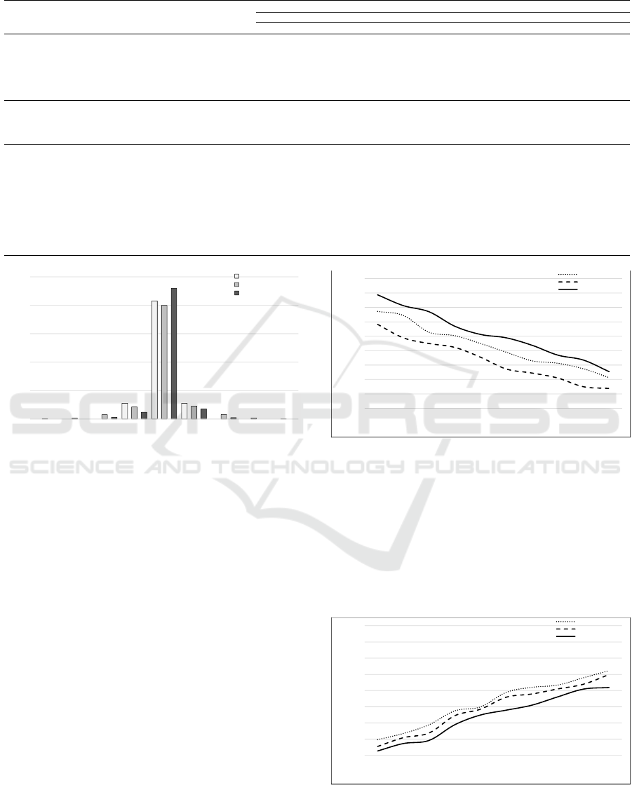
Table 1: PSNR/SSIM and embedding rate comparisons of other recent works and the proposed scheme.
Cover image
Lena Baboon AirplaneScheme category Scheme
PSNR (dB) SSIM bpp PSNR (dB) SSIM bpp PSNR (dB) SSIM bpp
(Lee and Huang, 2012) (2012) 22.32 0.867 1.32 21.24 0.651 1.32 23.76 0.797 1.34
(Lu, 2018) (2018) 40 - 1.2 35.99 - - 40 - 1.2
(Wahed and Nyeem, 2019) (2019) 46.88 0.9352 1.87 47.19 0.9922 1.88 39.55 0.914 1.445
(Shaik and V, 2019) (2019) 32.24 - 1.8 22.98 - 2.1 29.42 - 1.2
(Chen et al., 2020) (2020) 34.18 - 1.41 24.69 - 2.4 32.84 - 1.27
Interpolation based
(Hassan and Gutub, 2021) (2021) - - - 21.53 - 2.1 28.11 - 1.32
(Zhang et al., 2016) (2016) 36.3 - 0.25 37.5 - 0.25 37.8 - 0.25
(Zhang et al., 2019) (2019) 44 .41 - 0 .5 27 .11 - 0 .5 44 .94 - 0 .5
(Wu et al., 2021) (2021) 48 - 2.39 22 - 0.9 23 - 2.4
Encryption based
(Manikandan and Zhang, 2022) (2022) - - - 28.29 0.97 0.063 45.7 0.999 0.125
(Zhang and Wang, 2006) (2006) 51.8 0.9971 1.16 51.8 0.9989 1.16 51.79 0.9967 1.16
(Jung and Yoo, 2009) (2009) 47.92 0.9904 2.3 47.95 0.9975 2.3 47.97 0.9897 2.3
(Chao et al., 2009) (2009) 52.1 0.9965 1.85 46.3 0.9962 1.85 46.7 0.996 1.85
(Li and He, 2018) (2018) 42.74 - 2.1 36.63 - 2.6 43.23 - 2.1
(Liu et al., 2019) (2019) 51.8 - 1.16 - - - 51.54 1.15
(Kumar and Jung, 2020) (2020) 39.5 - 0.22 38.5 - 0.22 38.5 - 0.22
(Saha et al., 2020) (2020) 48.66 - 2 48.52 - 2 48.52 - 2
(Peng et al., 2020) (2020) 43.2 - 0.75 38.5 - 0.6 46.5 - 0.72
(Leng et al., 2021) (2021) 43.74 - 2.5 43.73 - 2.5 43.74 - 2.5
Modulus based
Proposed scheme 59.987 0.9992 2.49 59.321 0.9990 2.49 59.307 0.9994 2.49
0
0.5
1
1.5
2
2.5
-4 -3 -2 -1 0 +1 +2 +3 +4
x 10^5
EMD scheme
DE scheme
Proposed scheme
Figure 8: Average PVD histograms between cover images
and their stego images generated by the EMD, DE and pro-
posed schemes.
3.3.2 Salt and Pepper Noise Analysis
The robustness of a steganographic scheme in noisy
conditions is tested by introducing salt and pepper
noise. This noise alters certain pixels to either black
or white and is added to the stego images at vary-
ing intensities, ranging from 10% to 100%. Figure
9 shows the PSNR values for the corrupted stego im-
ages, where the stego images themselves are obtained
using the proposed scheme as well as that by using
the EMD and DE schemes. It is seen from this figure
that the proposed scheme provides the highest PSNR
values at all the levels of the noise indicating that the
attacker would be led to believe less that there is a se-
cret data hidden in the stego image produced by the
proposed scheme.
The bit error rate (BER) is defined as the propor-
tion of incorrectly extracted secret data bits to the total
number of bits embedded. A lower BER value signi-
fies a higher success rate in accurately extracting the
secret data, even when the stego image has been com-
promised by salt and pepper noise. Figure 10 illus-
trates the BER values for these noise-affected stego
10
12
14
16
18
20
22
24
26
28
10% 20% 30% 40% 50% 60% 70% 80% 90% 100%
PSNR (dB)
Noise densities
EMD scheme
DE scheme
Proposed scheme
Figure 9: Comparison of the average PSNR for salt and
pepper noisy images with noise densities.
images. These images were generated using the pro-
posed scheme and the existing EMD and DE schemes.
The data presented in this figure clearly indicates that
the proposed scheme consistently achieves the low-
est BER values across all levels of noise, highlighting
its superior performance in ensuring the accurate re-
trieval of secret data from corrupted stego images.
0
1
2
3
4
5
6
7
8
10% 20% 30% 40% 50% 60% 70% 80% 90% 100%
BER(%)
Noise densities
EMD scheme
DE scheme
Proposed scheme
Figure 10: Comparison of the average BER for salt and pep-
per noisy images with noise densities.
SECRYPT 2024 - 21st International Conference on Security and Cryptography
402
3.3.3 RS Analysis Attack
RS analysis attack detects hidden data in images by
analyzing the regular (Rm) and singular (Sm) groups
of pixels. This analysis evaluates the changes in
these groups before and after flipping the least signifi-
cant bits (LSBs), identifying irregularities that are in-
dicative of steganographic alterations (Fridrich et al.,
2001). Figure 11 illustrates the RS analysis results for
the proposed scheme applied to the cover image Lena.
The analysis suggests that the stego images exhibit no
signs of data concealed in their LSBs, as evidenced
by the closely matching expected values of the regu-
lar (Rm,R
′
) and singular (Sm, S
′
) pixel groups, both
with and without flipped LSBs. The ratios Rm/R
′
m
and Sm/S
′
m demonstrate a similarity characteristic
of unaltered images. Consequently, this strongly in-
dicates that the proposed steganographic scheme is
effective in concealing data, maintaining the natural
balance between the R and S groups (i.e., Rm
∼
=
R
′
m
and Sm
∼
=
S
′
m), thereby securing against RS analysis
attack.
0%
5%
10%
15%
20%
25%
30%
35%
40%
0% 10% 20% 30% 40% 50% 60% 70% 80% 90%
Embedding rate
Sm
S-m
Rm
R-m
Figure 11: RS-analysis yielded for Lena stego image gen-
erated by the proposed scheme.
4 FPGA IMPLEMENTATION:
RESULTS AND COMPARISONS
Embedded systems within FPGA platforms primar-
ily consist of a processing system (PS) and pro-
grammable logic (PL). The PS typically includes a
processor, system memory, and built-in peripherals,
while the PL provides flexibility for custom hard-
ware implementations. This combination facilitates
the development of highly customizable and effi-
cient embedded systems tailored to specific applica-
tions. Among the many FPGAs capable of host-
ing embedded systems, notable options include the
Nexys Video Artix-7 FPGA, AMD Xilinx Zynq-7000
SoC ZC706 Evaluation Kit, and the ZedBoard Zynq-
7000. Each of these boards has its own strengths,
with considerations such as image processing capa-
bilities, I/O expansions, processor performance, and
cost-effectiveness playing a crucial role in their selec-
tion. Given these criteria, the ZedBoard Zynq-7000
emerges as our chosen platform due to its balance of
hardware capability and affordability.
The ZedBoard specifically features the AMD Xil-
inx Z-7020 Zynq-7000 APSoC, which combines a
dual Cortex-A9 ARM processor operating at 866
MHz within its PS, and an Artix-7 FPGA in its PL.
This architecture not only supports advanced image
processing for steganographic applications but also
facilitates efficient communication between the PS
and PL via industry-standard AXI connections. The
fixed architecture of the PS, including essential pe-
ripherals and memory controllers, complements the
customizable nature of the PL, where the Artix-7
FPGA allows for the implementation of specialized
IP cores.
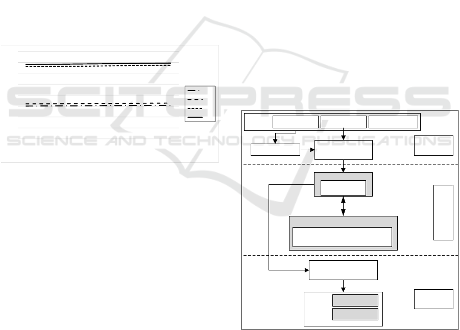
4.1 Overall System Architecture
In this paper, designing and implementing the pro-
posed steganographic scheme within this stegano-
graphic embedded system framework is essential.
Figure 12 illustrates the overall schematic flow of the
proposed reconfigurable Zynq-7000 APSoC for the
proposed steganographic scheme.
Extract pixels
Convert into hex
format file
Stego image
Output:
ZYNQ
-7000
APSoC part
MATLAB
part
MATLAB
part
PSPS
Convert into pixels/
hex format file
Secret data
PLPL
Steganographic scheme
(Algorithm 1)
Steganographic scheme
(Algorithm 1)
PL
Steganographic scheme
(Algorithm 1)
Cover image Secret dataInput:
Configurations
Cover image Secret dataInput:
Configurations
Dual core ARM
processor
Figure 12: General schematic flow of the proposed recon-
figurable Zynq-7000 APSoC (Algorithm 1).
The schematic follows a top-bottom flow, where
MATLAB is utilized for image representation and
pixel-hex format conversion. The embedding pro-
cess is as follows. (i) The Zynq-7000 APSoC plat-
form receives the cover image and the secret data as
High-Speed Pipelined FPGA Implementation of a Robust Steganographic Scheme for Secure Data Communication Systems
403
Shift register
FIFOFIFO
Secret data block B
Shift register
FIFOFIFO
Cover pixels
(Q
0
, Q
1
, Q
2
)
In data
Mode
Out data
6464
6464 646464
11
Lookup tables
construction
Stego pixels
(Q’
0
, Q’
1
, Q’
2
)
Stego pixels
(Q’
0
, Q’
1
, Q’
2
)
Cover pixels
(Q
0
, Q
1
, Q
2
)
(L
1,
L
2
)
Segments
Concealing secret digitsConcealing secret digits
Embed S
1
Embed S
2
Embed S
0
Embed S
1
Embed S
2
Embed S
0
Extracting secret digitsExtracting secret digits
Recover S
1
Recover S
2
Recover S
0
Recover S
1
Recover S
2
Recover S
0
S
0
S
1
S
2
S
0
S
1
S
2
S
0
S
1
S
2
S
0
S
1
S
2
Secret data block B
Stego pixels
(Q’
0
, Q’
1
, Q’
2
)
— Embedding
— Recovery
— Embedding
— Recovery
Figure 13: Hardware architecture of the steganographic scheme.
two separate inputs. (ii) MATLAB extracts the pixels
from the cover image and converts them into a hex
value file, along with the secret data. (iii) The recon-
figurable Zynq-7000 embedded system acquires this
file, containing the hex values of the image pixels and
the secret data, into its PS. (iv) The steganographic
scheme conceals the secret data within the hex values
of the image pixels. (v) MATLAB is used once again
to transform the modified hex values back into pixels,
generating the final stego image.
4.2 Proposed Hardware Architecture
The hardware architecture of the steganographic
scheme is depicted in Figure 13. A data block, com-
prising hex values of pixels and secret data, is sourced
from the DDR3 RAM to feed the IP core. As the input
FIFO becomes fully loaded, the embedding process
initiates. Once this begins, an interrupt signal is acti-
vated to denote that the IP core is currently occupied,
preventing further DDR3 RAM reads. Depending on
the Mode input signal, a shift register reads from the
input FIFO to either perform the embedding (conceal-
ing) or the recovery (extracting) of the secret data.
The hardware implementation of the stegano-
graphic scheme is carried out by implementing the
two processes: embedding and recovery, as well as
the two lookup tables. The lookup tables (LUTs) of
the Artix-7 FPGA device are utilized to facilitate the
weighted sum modulo functions of the EMD and DE
schemes. To enhance the performance of the architec-
ture, sub pipelining is employed to minimize the de-
lay in the critical path, a technique especially effective
for architectures with iterative behavior. By strate-
gically adding the optimal number of sub pipelining
stages, we strike an efficient balance between speed
and area. Figure 14 illustrates the trade-off between
delay and area for 1 to 4 sub pipelining stages within
our design. The optimal trade-off is realized with two
stages: the first inserted after the constructed lookup
tables and the second inserted after the weighted sum
modulo functions. To further refine timing perfor-
mance, a register balancing (retiming) strategy is in-
tegrated into the architecture.
0
1
2
3
4
5
0
100
200
300
400
500
1 2 3 4
Sub pipelining stages
Delay-to-area trade-off
LUTs
Slices
Delay (ns)
Figure 14: Delay-to-area (slices, LUTs) trade-off using dif-
ferent number of sub pipelining stages.
4.3 Place and Route Implementation
Results
The development of the steganographic IP core in-
volves three stages: design, implementation, and in-
tegration. Initially, RTL Verilog is used in the design
stage to craft an effective steganographic approach
tailored for FPGA use. This stage includes functional
and timing simulations with AMD Xilinx ISim to val-
idate design performance. Next, during implementa-
tion, these designs are synthesized and physically re-
alized on the FPGA, with a focus on optimizing re-
source use, speed, and power efficiency, utilizing the
Vivado tool for enhancements like register balancing
and logic optimization. A timing constraint ensures
an optimal trade-off between size and speed, aiming
for zero timing errors.
Table 2 presents the place and rout results of the
hardware implementation in comparison with other
recent FPGA steganographic implementations. The
proposed hardware implementation outperform oth-
SECRYPT 2024 - 21st International Conference on Security and Cryptography
404
Table 2: Comparison of the implemented scheme with other implementations (place and route results).
Scheme FPGA Slices FFs LUTs BRAMs
Freq. Throughput Power Image quality Embedding rate Processing rate
(MHz) (Mbps) (mW )* (PSNR) (bpp) ( f ps)
EMD-based (Shet et al., 2019) Artix-7 296 1890 1419 - 144.00 143.9 3807 45.6 1.16 549.00
Lifting-based (Phadikar et al., 2019) Artix-7 476 555 350 128 130.14 188.8 78.45 34.79 0.004 75.00
Parallelism-based (Seyed Dizaji et al., 2021) Virtex-6 - - - - 118.66 - - 42.99 0.26 -
Threshold-based (Wei et al., 2021) Spartan-6 - 670 627 7 - - 200 44.43 0.25 -
LSB matching (Sinha Roy et al., 2021) Spartan-3A - 647 668 - - - 369.3 51.37 1.00 -
Chaotic-based (Sun et al., 2023) Cyclone IV 1100 537 1067 - - - - 53.24 2.00 -
Template-based (Dzhanashia and Evsutin, 2023) Artix-7 - - - 1 120 13.516 2450 39.66 0.00097 8.593
Our design Artix-7 148 523 320 2 289.7 2318 152 81.92 5.52 1054.07
* The values given are the powers consumed by only the PL parts of the various hardware implementations.
ers in speed, resource utilization, throughput, and
power consumption. The enhanced performance is at-
tributed to the sub pipelining applied in the hardware
architecture of the steganographic scheme. Power
consumption is assessed using the AMD Xilinx power
estimator (XPE) tool, with values in Table 2 repre-
senting only the PL part (FPGA device). Notably, our
design is ideal for low-power, resource-limited de-
vices such as wearables and RFIDs, given its compact
footprint. Efficiency is evident in the operating speed
to LUT ratio, at 0.905, surpassing the previous best
of 0.10 reported in (Shet et al., 2019). Furthermore,
our hardware implementation achieves a throughput
to LUT ratio of 7.24, which is higher than the 0.54
reported in (Phadikar et al., 2019).
In the integration phase, the implemented design
is packaged as an IP core using the AMD Xilinx IP
package integrator. This tool is used to rapidly con-
nect the design, implemented on PL, to PS using the
AXI4 interface. The image steganographic system
using the Zynq-7000 APSoC has four IP cores con-
nected to PS in the Zynq-7000 APSoC. The stegano-
graphic IP core is considered a custom core and can
be modified to add more features and support more
functions. The UART and I/O IP cores, on the other
hand, are produced by AMD Xilinx.
To achieve real-time steganographic performance,
modulo arithmetic for data embedding is executed on-
the-fly by a dedicated, optimized IP core on the AMD
Xilinx Zynq-7000 APSoC. The stego images are gen-
erated instantly as cover images and secret data are
received, with a library of cover images pre-loaded in
DDR3 RAM to eliminate delays. The processing sys-
tem (PS) utilizes two buffers to manage the flow of
images and data to and from the DDR3 RAM, facil-
itating fast, cyclic processing by the steganographic
core. This core also supports parallel processing, en-
hancing the system’s speed. These measures result in
a high-performance steganographic system with supe-
rior speed, efficiency, and lower power consumption,
surpassing other hardware implementations.
5 CONCLUSIONS
This paper introduces a novel steganographic scheme
implemented on the AMD Xilinx Zynq-7000 AP-
SoC hardware platform. It features an integrated
IP core that significantly enhances efficiency, speed,
and power consumption. The design demonstrates
superior operating speed, resource utilization, and
throughput compared to recent hardware steganogra-
phy solutions, making it ideally suited for real-time
processing and secure data communication applica-
tions.
ACKNOWLEDGMENTS
This work was supported in part by the Natural Sci-
ences and Engineering Research Council (NSERC) of
Canada and in part by the Regroupement Strategique
en Microelectronique du Quebec (ReSMiQ).
REFERENCES
Chao, R.-M., Wu, H.-C., Lee, C.-C., and Chu, Y.-P. (2009).
A Novel Image Data Hiding Scheme with Diamond
Encoding. EURASIP Journal on Information Security,
2009(1):658047.
Chen, Y.-q., Sun, W.-j., Li, L.-y., Chang, C.-C., and Wang,
X. (2020). An efficient general data hiding scheme
based on image interpolation. Journal of Information
Security and Applications, 54:102584.
Dzhanashia, K. and Evsutin, O. (2023). FPGA implementa-
tion of robust and low complexity template-based wa-
termarking for digital images. Multimedia Tools and
Applications.
Fakhredanesh, M., Rahmati, M., and Safabakhsh, R.
(2019). Steganography in discrete wavelet transform
based on human visual system and cover model. Mul-
timedia Tools and Applications, 78(13):18475–18502.
Fridrich, J., Goljan, M., and Du, R. (2001). Reliable detec-
tion of lsb steganography in color and grayscale im-
ages. In Proceedings of the 2001 Workshop on Mul-
timedia and Security: New Challenges, page 27–30.
Association for Computing Machinery.
High-Speed Pipelined FPGA Implementation of a Robust Steganographic Scheme for Secure Data Communication Systems
405

Hassan, F. S. and Gutub, A. (2021). Efficient Image Re-
versible Data Hiding Technique Based on Interpola-
tion Optimization. Arabian Journal for Science and
Engineering, 46(9):8441–8456.
Jung, K.-H. and Yoo, K.-Y. (2009). Improved Exploiting
Modification Direction Method by Modulus Opera-
tion. International Journal of Signal Processing, Im-
age Processing and Pattern, 2:11.
Kumar, R. and Jung, K.-H. (2020). Robust reversible data
hiding scheme based on two-layer embedding strat-
egy. Information Sciences, 512:96–107.
Kumar, V. and Kumar, D. (2018). A modified DWT-based
image steganography technique. Multimedia Tools
and Applications, 77(11):13279–13308.
Kuo, W.-C., Wang, C.-C., and Hou, H.-C. (2016). Signed
digit data hiding scheme. Information Processing Let-
ters, 116(2):183–191.
Lee, C.-F. and Huang, Y.-L. (2012). An efficient image in-
terpolation increasing payload in reversible data hid-
ing. Expert Systems with Applications, 39(8):6712–
6719.
Leng, H.-S., Lee, J.-F., and Tseng, H.-W. (2021). A
high payload EMD-based steganographic method us-
ing two extraction functions. Digital Signal Process-
ing, 113:103026.
Li, Z. and He, Y. (2018). Steganography with pixel-
value differencing and modulus function based on
PSO. Journal of Information Security and Applica-
tions, 43:47–52.
Liu, Y.-X., Yang, C.-N., Sun, Q.-D., Wu, S.-Y., Lin, S.-S.,
and Chou, Y.-S. (2019). Enhanced embedding capac-
ity for the SMSD-based data-hiding method. Signal
Processing: Image Communication, 78:216–222.
Lu, T.-C. (2018). Interpolation-based hiding scheme using
the modulus function and re-encoding strategy. Signal
Processing, 142:244–259.
Mandal, P. C., Mukherjee, I., Paul, G., and Chatterji, B. N.
(2022). Digital image steganography: A literature sur-
vey. Information Sciences, 609:1451–1488.
Manikandan, V. M. and Zhang, Y.-D. (2022). An adaptive
pixel mapping based approach for reversible data hid-
ing in encrypted images. Signal Processing: Image
Communication, 105:116690.
Peng, F., Zhao, Y., Zhang, X., Long, M., and Pan, W.-q.
(2020). Reversible data hiding based on RSBEMD
coding and adaptive multi-segment left and right his-
togram shifting. Signal Processing: Image Communi-
cation, 81:115715.
Phadikar, A., Maity, G. K., Chiu, T.-L., and Mandal, H.
(2019). FPGA Implementation of Lifting-Based Data
Hiding Scheme for Efficient Quality Access Control
of Images. Circuits, Systems, and Signal Processing,
38(2):847–873.
Saha, S., Chakraborty, A., Chatterjee, A., Dhargupta, S.,
Ghosal, S. K., and Sarkar, R. (2020). Extended ex-
ploiting modification direction based steganography
using hashed-weightage Array. Multimedia Tools and
Applications, 79(29):20973–20993.
Seyed Dizaji, S. H., Zolfy Lighvan, M., and Sadeghi, A.
(2021). Hardware-Based Parallelism Scheme for Im-
age Steganography Speed up. In Proc. International
Conference on Innovative Computing and Communi-
cations, Advances in Intelligent Systems and Comput-
ing, pages 225–236, Singapore. Springer.
Shaik, A. and V, T. (2019). High capacity reversible data
hiding using 2D parabolic interpolation. Multimedia
Tools and Applications, 78(8):9717–9735.
Shet, K. S., Aswath, A. R., Hanumantharaju, M. C.,
and Gao, X.-Z. (2019). Novel high-speed recon-
figurable FPGA architectures for EMD-based image
steganography. Multimedia Tools and Applications,
78(13):18309–18338.
Sinha Roy, S., Basu, A., Chattopadhyay, A., and Das, T. S.
(2021). Implementation of image copyright protection
tool using hardware-software co-simulation. Multime-
dia Tools and Applications, 80(3):4263–4277.
Sukumar, A., Subramaniyaswamy, V., Ravi, L., Vijayaku-
mar, V., and Indragandhi, V. (2021). Robust image
steganography approach based on RIWT-Laplacian
pyramid and histogram shifting using deep learning.
Multimedia Systems, 27(4):651–666.
Sun, J.-y., Cai, H., Gao, Z.-b., Wang, C.-p., and Zhang, H.
(2023). A novel non-equilibrium hyperchaotic sys-
tem and application on color image steganography
with FPGA implementation. Nonlinear Dynamics,
111(4):3851–3868.
Wahed, M. A. and Nyeem, H. (2019). Reversible data hid-
ing with interpolation and adaptive embedding. Mul-
timedia Tools and Applications, 78(8):10795–10819.
Wei, J., Quan, Z., Hu, Y., Liu, J., Zhang, H., and Liu, M.
(2021). Implementing a Low-Complexity Steganogra-
phy System on FPGA. In Proc. 9th International Con-
ference on Intelligent Computing and Wireless Optical
Communications (ICWOC), pages 64–68.
Wu, F., Zhou, X., Chen, Z., and Yang, B. (2021). A re-
versible data hiding scheme for encrypted images with
pixel difference encoding. Knowledge-Based Systems,
234:107583.
Zhang, R., Lu, C., and Liu, J. (2019). A high capacity
reversible data hiding scheme for encrypted covers
based on histogram shifting. Journal of Information
Security and Applications, 47:199–207.
Zhang, X., Long, J., Wang, Z., and Cheng, H. (2016).
Lossless and Reversible Data Hiding in Encrypted Im-
ages With Public-Key Cryptography. IEEE Transac-
tions on Circuits and Systems for Video Technology,
26(9):1622–1631.
Zhang, X. and Wang, S. (2006). Efficient Stegano-
graphic Embedding by Exploiting Modification Di-
rection. IEEE Communications Letters, 10(11):781–
783.
SECRYPT 2024 - 21st International Conference on Security and Cryptography
406
