
Revolutionizing Wireless Communication: The Convergence of
CNT and Antennas for Futuristic THz Communication
Atanu Chowdhury
1a
and Soumya Sen
2b
1
Calcutta Institute of Technology, Uluberia, West Bengal, India
2
University of Engineering & Management, Jaipur, Rajasthan, India
Keywords: THz Communication, Nano-Antenna, CNT, High Gain.
Abstract: This manuscript presents a circular patch Carbon Nano Tube (CNT) antenna having two “Z” slots and a
defected ground structure (DGS) suitable for optical frequency applications. A semi-spherical layer of the
Polyflon Cuflon layer(ε
r
=3.41) is attached to the ground to enhance the gain resulting in an improvement in
radiation efficiency. The proposed antenna dimension is 40 nm × 40 nm × 1.6 nm based upon a silicon substrate
(ε
r
=11). The proposed antenna covers a bandwidth of 2 THz to 6.5 THz. Without the attached layer, the
maximum gain is 3.5 dB while the attachment of the layer increases it up to 6.1 dB. The Radiation efficiency
is also improved from 62% to 81% by implementing the attachment. The overall structure is designed and
simulated in HFSS 21.0 software.
1
INTRODUCTION
Microwave researchers are currently focusing on
modern communication technologies and modulation
techniques to address bandwidth challenges, aiming
to enhance spectral utilization efficiency (PAULRAJ
et al., 2004). These efforts also target improvements
in data rates and frequency reuse. However, Shan-
non’s theory imposes an upper limit on channel ca-
pacity, even with advancements like MIMO
technology. To overcome this limitation, researchers
are considering higher bands applicable for optical
frequency range communication, such as the band of
1000 MHz to 10 THz (Akyildiz et al., 2014).
Recently, a “bow- tie” antenna has been optimized
for communicating in between 110-292 THz,
utilizing a glass as the base and an aluminium dipole
antenna to optimize parameters (Kavitha et al.,
2023).
Despite its potential, THz signal usage lags
behind that of the electrical or optoelectronic field
due to hardware limitations, particularly in THz
signal generators and sensors. However, since the
1980s, the accessibility of nanosecond lasers and
photo-conductive antennas has enabled several
fields, like medical science, pharmaceutical-
a
https://orcid.org/0000-0002-9323-4839
b
https://orcid.org/0000-0002-6354-5206
oriented research, and also pri- vacy, to utilize THz
waves (Apriono et al., 2015; Car-valho et al., 2023).
The advantages of THz communi- cation include
enhanced directionality, data security, and reduced
attenuation (Federici and Moeller, 2010).
Nevertheless, higher atmospheric absorption limits its
utility for short-distance communication. Despite
high demand over the last 2 decades, hardware imple-
mentation for THz frequency range operation remains
challenging.
In the realm of THz services, recent developments
in- volve the creation of various metal-fabricated
nano- antennas and array orientations, such as lens
antennas, horn antennas and many more (Malhotra et
al., 2017; Konstantinidis et al., 2015; Alazemi et al.,
2016; Yu et al., 2020; Hao et al., 2017). Fabricating
these high-frequency antennas poses challenges due
to measurements in the nanometer range. Con-
sequently, researchers are exploring alternative
materials like graphene and carbon nanotubes to
mitigate skin depth reduction associated with
traditional materials like gold and copper. Recent
studies have compared antenna materials and their
performances for THz communication nanoantenna
designs (Ghaf- far et al., 2019).
Moreover, simulations of an antenna optimized
by a silicon lens having a silicon substrate have
shown promise, with additional layers applied to the
lens surface to boost effectiveness (Dash et al.,
Chowdhury, A. and Sen, S.
Revolutionizing Wireless Communication: The Convergence of CNT and Antennas for Futuristic THz Communication.
DOI: 10.5220/0013231800004646
Paper published under CC license (CC BY-NC-ND 4.0)
In Proceedings of the 1st International Conference on Cognitive & Cloud Computing (IC3Com 2024), pages 25-29
ISBN: 978-989-758-739-9
Proceedings Copyright © 2025 by SCITEPRESS – Science and Technology Publications, Lda.
25
2020). Researchers are also examining broadband
imple- mentations using the bow-tie antenna in
conjunction with capacitive lines and a hemispherical
silicon lens. However, further enhancements in
electromagnetic properties are needed to improve
radiation effective- ness (Wahyudi et al., 2017).
Research indicates that a silicon lens is useful for the
enhancement of the di- rectional capability of a light-
conducting antenna on a Galium Arsenite base within
the THz spectrum range (Jyothi et al., 2016).
Additionally, ”bow-tie” antennas on a surface made
of InP, combined with hemispheri- cal and bullet-type
silicon lenses, have been utilized to eliminate surface
waves, resulting in improved gain, efficiency, and a
wider spectrum (Li and Song, 2016). This research
article introduces a novel concept: A circular patch
antenna with two ”Z” slots and a de- fected ground
structure (DGS) has been developed for optical
frequency applications. To enhance its gain and
radiation efficiency, a semi-spherical layer of
Polyflon Cuflon material (with a relative permittivity
of 3.41) is attached to the ground. The antenna is
designed with dimensions of 40 nm × 40 nm × 1.6
nm on a silicon substrate with a relative permittivity
of 11. It operates within a bandwidth ranging from 2
THz to 6.5 THz.
Before attaching the layer, the antenna achieves a
maximum gain of 3.5 dB. However, with the attached
layer, the gain increases significantly to 6.1 dB. Addi-
tionally, the radiation efficiency improves from 62%
to 81% with the implementation of the attached layer.
The entire structure is designed and simulated using
HFSS 21.0 software.
2
ANTENNA DESIGN &
ANALYSIS
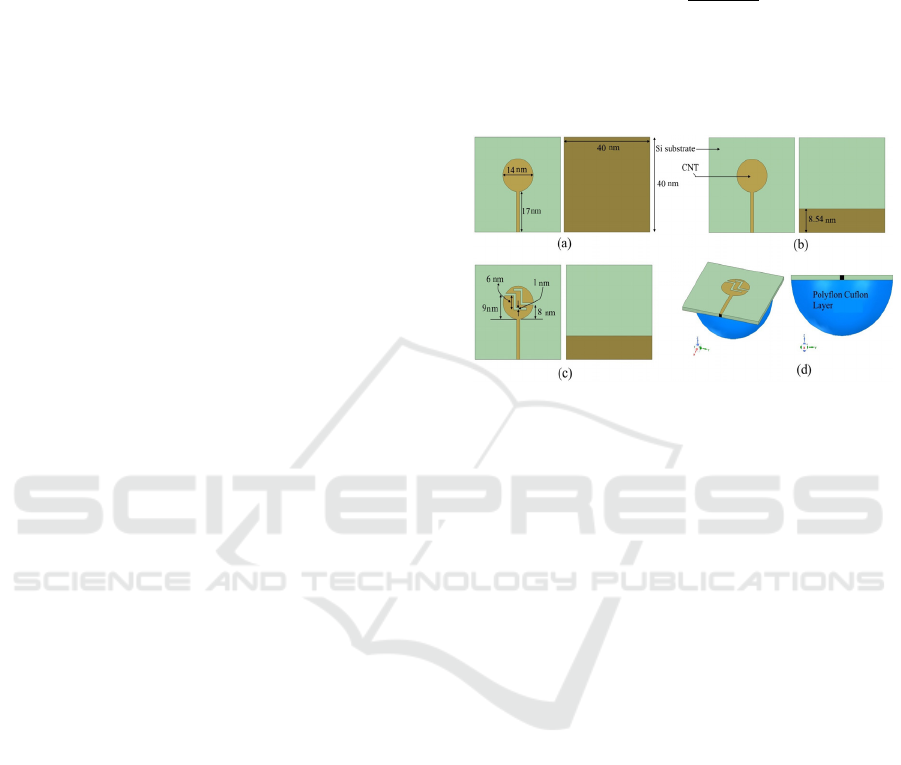
The proposed antenna is designed in a few steps on
the silicon substrate. The volume of the substrate is
40 nm × 40 nm × 1.6 nm. In step-1, a simple
circular horizontally aligned CNT patch antenna
is designed with a radius of 7 nm and a feedline
having a length of 17 nm, and a width of 2 nm. This
structure is shown in Fig. 1(a). In step-2, the ground
is defected to a rectangular shape as shown in
Fig.1(b). In step-3, the circular patch is slotted with
two “Z”-slots to enhance the coverage of the
frequency band as shown in Fig. 1(c). In step-4, a
layer of Polyflon Cuflon (ε
r
=3.41) is attached to the
ground as shown in Fig. 1(d). This is done to
increase the gain as well as efficiency. As we all
know the dielectric constant of the silicon substrate
(ε
r
) and air is 11 and 1 respectively. To counter this
gap between these dielectric layers, a matching layer
was needed. So, mathematically a layer is to be
introduced whose dielectric constant can be found
from the equation (1).
𝜀
=
𝜀
× 𝜀
(1)
This equation gives a value of around 3.4058.
This is why, a material is so chosen whose dielectric
constant is 3.41 i.e. Polyflon Cuflon.
Figure 1: Antenna designs in different steps: Top view and
Bottom view in (a) step-1, (b) step-2, (c) step-3, (d) step-4
(optimized).
3
RESULTS
3.1
S-Parameter
The S(1,1) parameter is studied to determine the
return loss. It is significant to obtain the bandwidth
of the antenna. In this study, the S(1,1) parameter is
discussed for all the design steps involved to get the
optimized value as given in Fig. 2. In the first step, it
is from 3.3 THz to 5.1 THz. In step-2, it is improved
from 2.6 THz to 5.6 THz. In the next one, it provides
a bandwidth of 2.4 THz to 6 THz. And finally, after
the implementation of the said layer, the obtained
bandwidth is from 2 THz to 6.5 THz.
3.2
Radiation Pattern
The S(1,1) parameter result has provided two
resonant frequencies in the obtained band.
These
are 3.4 THz and 4.6 THz. The radiation pattern of
these frequencies is shown in Fig. 3 and Fig. 4
respectively. It shows a pattern uniformly distributed
in each direction while the phase angles are 0
0
, 90
0
.
IC3Com 2024 - International Conference on Cognitive & Cloud Computing
26
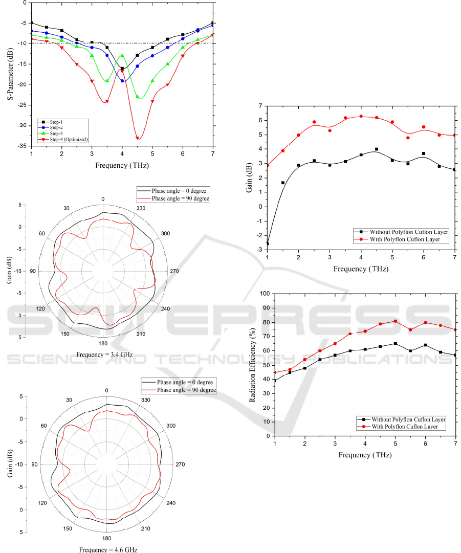
Figure 2: Reflection Co-efficient.
Figure 3: Radiation Pattern at 3.4 THz.
Figure 4: Radiation Pattern at4.6 THz.
3.3
Gain & Efficiency
In this section, the gain, and efficiency are studied.
This section shows how the Polyflon Cuflon affects
the performance of the antenna. Fig.5 and Fig.6
show the gain and efficiency of the proposed
antenna respectively. These show that without the
attached layer, the maximum gain is 3.5 dB while the
attachment of the layer increases it up to 6.1 dB. The
Radiation efficiency is also improved from 62% to
81% by implementing the attachment.
Figure 5: Gain of the proposed nano-antenna.
Figure 6: Radiation Efficiency of the proposed nano-
antenna.
4
COMPARISON
The proposed work is compared with recent
literature in Table 1.
Revolutionizing Wireless Communication: The Convergence of CNT and Antennas for Futuristic THz Communication
27

Table 1: Table of Performance Evaluation.
References
Dimension
(
nm
3
)
B/W
(THz)
Max.
Eff.
(%)
Alazemi, 2016 46×24×0.432 0.4
N
P
Yu, 2020 10×6.7×1.5 0.3 99.5
Dash, 2020
N
P 1 93.7
Wahyudi, 2017 6×6×0.3 0.3 90
Jyothi, 2016 1.2×1.2×0.625 2 75
Li, 2016
N
P 1 90
T
W
40×40×1.6 4.5 82
5
CONCLUSION
The design of the antenna is elaborated in steps in
this paper. The compact size of the antenna is one
of the significant parts of this work. The band-
width achieved is 4.5 THz (2 to 6.5 THz) with a
maximum efficiency is 82% and a maximum gain
is about 6.1 dB. This antenna covers the full band
of the optical frequency. The performance
improvement is also studied using a matching layer
(Polyflon Cuflon). It shows a new way to improve
the antenna performance.
Advancements in fabrication techniques
promise to revolutionise multiple technological
sectors through the development of nanoantennas.
These techniques will allow for precise control
over dimensions and materials, consequently
enhancing performance and efficiency. Nano
antennas hold potential across a spectrum of
applications including communication
technologies, sensing, imaging, and energy
harvesting. Breakthroughs in terahertz technology
and meta-material development are anticipated,
further amplifying their impact. Ongoing research
and innovation in this field are poised to unlock
transformative applications in electronics,
telecommunications, and beyond.
ACKNOWLEDGEMENTS
Both authors express their heartiest
acknowledgement to themselves, their
organizations and ultimately to the god for the
completion of the research work.
REFERENCES
Akyildiz, I. F., Jornet, J. M., and Han, C. (2014). Ter-
ahertz band: Next frontier for wireless communica-
tions. Physical Communication, 12:16–32.
Alazemi, A. J., Yang, H.-H., and Rebeiz, G. M.
(2016). Double bow-tie slot antennas for wideband
millimeter-wave and terahertz applications. IEEE
Transactions on Terahertz Science and Technology,
6(5):682–689.
Apriono, C., Rahardjo, E., and Hiromoto, N. (2015). A
new method for simulating power flow density fo-
cused by a silicon lens antenna ir-radiated with lin-
early polarized thz wave. Makara Journal of Technol-
ogy, 19(2):59–64.
Carvalho, R., Brito-Pereira, R., Pereira, N., Lima, A. C.,
Ribeiro, C., Correia, V., Lanceros-Mendez, S., and
Martins, P. (2023). Improving the performance of
paper-based dipole antennas by electromagnetic flux
concentration. ACS Applied Materials & Interfaces,
15(8):11234–11243.
Dash, S., Liaskos, C., Akyildiz, I. F., and Pitsillides, A.
(2020). Nanoantennas design for thz communication:
material selection and performance enhancement. In
Proceedings of the 7th ACM International
Conference on Nanoscale Computing and
Communication, NanoCom ’20, New York, NY,
USA. Association for Computing Machinery.
Federici, J. and Moeller, L. (2010). Review of terahertz
and subterahertz wireless communications. Journal
of Applied Physics, 107(11).
Ghaffar, A., Li, X. J., Seet, B.-C., Awan, W. A., and
Hus- sain, N. (2019). Compact multiband frequency
reconfigurable antenna for 5g communications. In
2019 29th International Telecommunication
Networks and Applications Conference (ITNAC),
pages 1–3.
Hao, Z.-C., Wang, J., Yuan, Q., and Hong, W. (2017).
Development of a low-cost thz metallic lens antenna.
IEEE Antennas and Wireless Propagation Letters,
16:1751–1754.
Jyothi, A., Saha, C., Ghosh, B., Kini, R., and Vaisakh, C.
(2016). Design of a gain enhanced thz bow-tie photo-
conductive antenna. In 2016 International
Symposium on Antennas and Propagation (APSYM),
pages 1–3.
Kavitha, S., Sairam, K., and Singh, A. (2023).
Plasmonic equi-triangular slot loaded bowtie nano-
antenna for quantum optical wireless
communication. Photonics and Nanostructures -
Fundamentals and Applications, 55:101153.
Konstantinidis, K., Feresidis, A. P., Tian, Y., Shang, X.,
and Lancaster, M. J. (2015). Micromachined terahertz
fabry perot cavity highly directive antennas. IET
Microwaves, Antennas & Propagation, 9(13):1436–
1443.
Li, Y. and Song, R. (2016). A high gain on-chip tera-
hertz antenna with high efficiency. In 2016 IEEE
9th UK-Europe-China Workshop on Millimetre Waves
IC3Com 2024 - International Conference on Cognitive & Cloud Computing
28

and Terahertz Technologies (UCMMT), pages 222–
224.
Malhotra, I., Jha, K. R., and Singh, G. (2017).
Analysis of highly directive photoconductive dipole
antenna at terahertz frequency for sensing and
imaging applications. Optics Communications,
397:129–139.
PAULRAJ, A., GORE, D., NABAR, R., and
BOLCSKEI, H. (2004). An overview of mimo
communications - a key to gigabit wireless.
Proceedings of the IEEE, 92(2):198–218.
Wahyudi, T., Apriono, C., Zulkifli, F. Y., and Rahardjo, E.
T. (2017). Broadband planar bow-tie antenna on high
re- sistivity silicon substrate for terahertz application.
In 2017 15th International Conference on Quality in
Re- search (QiR) : International Symposium on
Electrical and Computer Engineering, pages 372–
376.
Yu, H.-y., Yu, J., Yao, Y., Liu, X., and Chen, X. (2020).
Wideband circularly polarised horn antenna with large
aspect ratio for terahertz applications. Electronics
Letters, 56(1):11–13.
Revolutionizing Wireless Communication: The Convergence of CNT and Antennas for Futuristic THz Communication
29
