
Optimized Sample and Hold Design Leveraging MOSFETs Using SPICE
Simulation
Soumya Sen
1a
, Atanu Chowdhury
2b
, Subarna Mondal
3c
and Agnibha Dasgupta
4d
1
University of Engineering & Management, Jaipur, Rajasthan, India
2
Calcutta Institute of Technology, Uluberia, West Bengal, India
3
National Institute of Technology, Durgapur, West Bengal, India
4
DIG Grid Support, GE Vernova, U.S.A.
Keywords: MOSFET, Digital-to-Analog Converter, Drain Induced Barrier Lowering, Sample and Hold (S/H) Circuit.
Abstract: In order to reduce research, it emphasizes building a diminished-distortion sample and hold circuit,
highlighting the importance of the MOSFET’s gate-to-source voltage being independent of the input. The
circuit that is being demonstrated here runs quickly and doesn’t require an operational amplifier, which
lowers power con- sumerism. Additionally, it harnesses the convenience of closely aligning transistor device
S1 to the switching device, restricting distortion and mitigating drain-induced barrier lowering (DIBL)
concerns. In linear plat- forms, sample and hold circuits are essential, particularly in some analog-to-digital
converters. These con- verters generate a voltage inside and measure it versus the input voltage through a
digital-to-analog converter (DAC). The input voltage uniformity is very important for precise adjustments
during this test. The conversion phase ends when the voltages are accurately replicating the initial input and
fall below a certain error limit.
1
INTRODUCTION
An analog device essential to electronic systems is
the sample and hold circuit. The ADC is used to
take a snapshot of the voltage of a constantly varying
analog signal.
Essentially, its analog memory task is to bring
the sample value and hold it for a defined period, but
mainly, we can say to keep the sample. These circuits
have applications in several electronic circuits, espe-
cially ADCs, used with devices like Peak detectors.
The sample and hold circuits are mostly included in
ADCs to handle issues caused by fluctuations in the
analog input signal. The analog-to-digital converter
transforms the analog input signal into a variable dig-
ital signal that may produce signal faults. Conse-
quently, the variation sources mentioned above are in-
deed greatly minimized by the actuality of the sample
and hold circuit because it takes a steady representa-
tion of the analog signal at the beginning of the con
version. When established as the reference standard,
a
https://orcid.org/0000-0002-6354-5206
b
https://orcid.org/0000-0002-9323-4839
c
https://orcid.org/0009-0004-8048-585X
d
https://orcid.org/0009-0000-1995-6019
this value enhances the precision and reliability of the
electrical devices that employ analog-to-digital
conversion methods in signal conditioning. (Iizuka et
al., 2018), (P. and Jacob, 2022), (Li et al., 2022),
(Gupta et al., 2022).
2
PROPOSED ARCHITECTURAL
METHODOLOGY
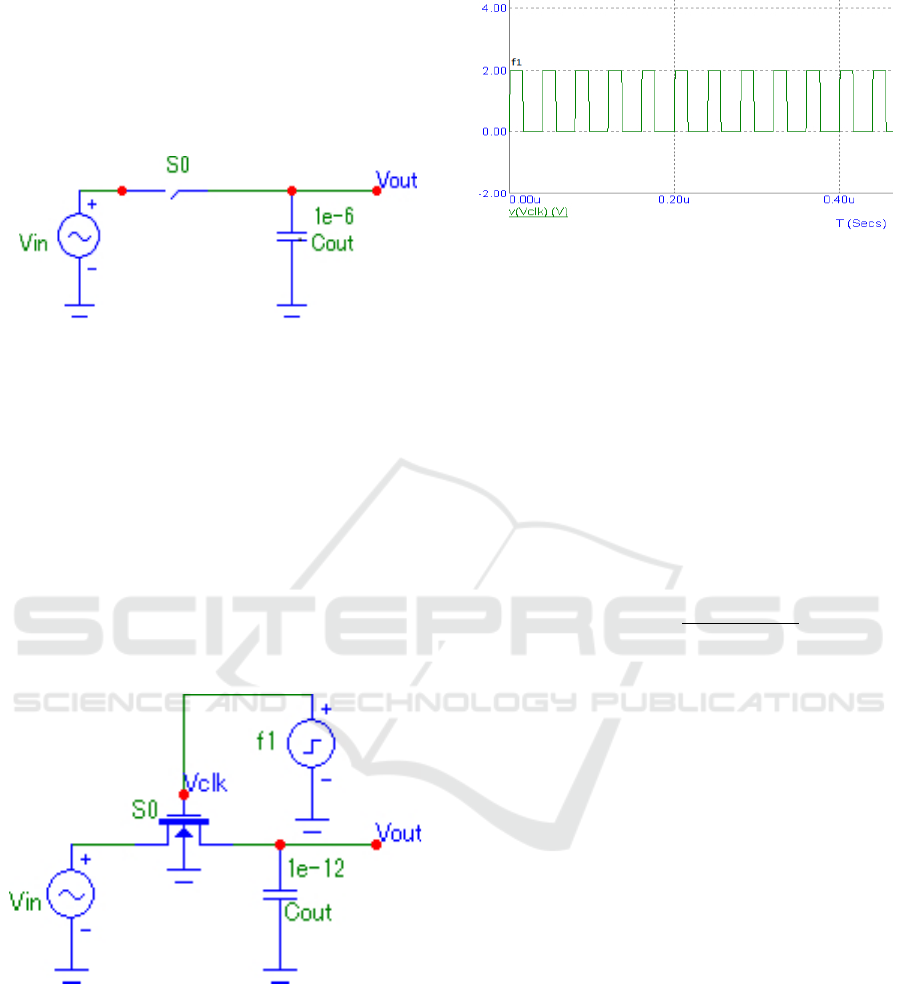
The block diagram of a typical sample and hold
circuit is shown in Figure 1. In this circuit, a switch
marked S0 is linked in sequence with a capacitor
labeled Cout. When the system is operating, the
voltage across the capacitor Cout is equal to the input
voltage Vin, and the switch S0 is engaged at the
sampling level.
As discussed in this paper, the modification pro-
posed to the conventional NMOS sample and hold
circuit is depicted in Figure 2. A control NMOS
transistor replaces the switch S0 of the conventional
structure in the design. This particular application
of semiconductor technology considers the unique
char- acteristics of NMO S transistors. Tanner Tool,
Sen, S., Chowdhury, A., Mondal, S. and Dasgupta, A.
Optimized Sample and Hold Design Leveraging MOSFETs Using SPICE Simulation.
DOI: 10.5220/0013278200004646
Paper published under CC license (CC BY-NC-ND 4.0)
In Proceedings of the 1st International Conference on Cognitive & Cloud Computing (IC3Com 2024), pages 85-89
ISBN: 978-989-758-739-9
Proceedings Copyright © 2025 by SCITEPRESS – Science and Technology Publications, Lda.
85
which specifically is a tool that has a special ability
to ana- lyze circuits, is used in the simulation and
analysis of the circuit. These core attributes of the
NMOS MOS- FETs used to implement the circuit
include width val- ues of 15µm, length values of
1.5µm, and a threshold voltage of 1.30 volts.
Figure 1: Conventional Sample and Hold Circuit Diagram.
The timing diagram in Figure 3 incorporates
every signal in the circuit, and details are given
concerning the pulse f1 to emphasize the temporal
characteris- tics of the circuit. When an NMOS
transistor is sub- jected to the sample and holds
circuit timing interac- tion is complex and is
depicted when input is applied to the gate. The time
base also gives important points and changes that are
meaningful and give information about the dynamic
data of the NMOS sample and hold circuit.
(Velagaleti et al., 2019), (D and Beulet, 2018),
(Heußen et al., 2023), (Kim et al., 2019), (Huang
et al., 2023).
Figure 2: NMOS-based S/H circuit.
A proper transfer of signals of capacitor Cout
towards the input is achieved when the switch is
closed and clock signal f
1
rises to high value (V
DD
) at
the gate of the switch. The input voltage is sampled
onto the capacitor if the NMOS is in its sampling
mode which is a mode of NMOS operation.
Figure 3: Schematic for the first pulse timing.
It is essential to make this change into triode
mode to get S0 into tracking mode. In this mode,
certain conditions must be met: the gate-to-source
voltage (V
gs
) should exceed the threshold voltage
(V
th
), and simultaneously, the drain-to-source
voltage (V
ds
) must remain less than the difference
between V
gs
and V
th
. Achieving these conditions
ensures proper functionality in tracking mode,
allowing the switch to follow the input signal
accurately.
The specific expression governing the gate-to-
source voltage is denoted as
V
gs
=
V
DD
−
V
in
(1)
R
on
=
1
µnCoxWL−1(Vgs −Vth)
(2)
When the input goes low, the switch turns off,
holding the input voltage on the capacitor and
placing the NMOS in hold mode. NMOS is chosen
over PMOS for the sample and hold circuit due to
advantages such as higher electron mobility, half
the on-resistance compared to PMOS, and a speed
advantage with smaller junction areas.
Despite the simplicity of the circuit in Fig.1.2,
turning off switch S0 leads to channel charge ac-
cumulation on the hold capacitor, causing output
voltage distortion. The gate-source voltage (V
gs
) and
threshold voltage (V
th
) of switch S0 are necessary to
determine the sampling instant. One method used to
lessen the repercussions of the input voltage on V
gs
is
to start rebooting. A bootstrapped sample and hold
circuit with an NMOS switch S0 and a hold capacitor
Cout is illustrated in Figure 4(a). The transistor’s
gate is anchored to a bootstrap circuit that consists
of switches S2 through S5 and capacitor C
bias
. The
timing sequence for waveforms f1 and f2 is shown
in Figure 4(b). C
bias
charges against the bias voltage
V
bias
during the initial phase ( f
1
strong). C
biasis
was
then injected to switch S0’s source and gate contacts
during the second phase ( f
2
strong). Therefore, the
V
gs
is depicted by
IC3Com 2024 - International Conference on Cognitive & Cloud Computing
86
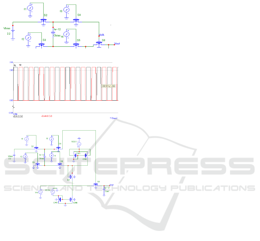
V
gs
= (V
bias
+V
in
) −V
in
= V
DD
(3)
(a)
(b)
(c)
Figure 4: (a) S/H circuit – Bootstrapped; (b) Timing
schematic for pulse f1 and f2; (c) Recommended design of
Sample and Hold Circuit.
Figure 4(c) illustrates a sampling transistor S0
and a hold capacitor Cout, both of which are NMOS
transistors. The transistor S1 is an NMOS transistor
configured as a diode. In this setup, an NMOS tran-
sistor has its drain connected to its gate. Transistor
S1 should ideally have the same sensitivity type as
transistor S0. Transistors CM1 and CM2, as well as
CM3 and CM4, form two current sources that control
the flow of current through transistor S1. Current
mirrors can be used to construct these current sources.
Switches S2 and S3 are active during the initial
stage of operation because switch signal f1 is high.
Switches S4 and S5 remain open because the switch
signal f2 is low at the same time. It is possible to
modify the switch signals f1 and/or f2 in accordance
with the type of switches being used. In this first
phase, the bootstrap capacitor Cbias has a voltage
of Vbias across it, as Figure 1.4(c) illustrates. The
bootstrapping capacitor Cbias is connected to the
gate of the transistor S0 and placed in series with
transistor S1 during the second phase when f1 is low,
and f2 is high. As a result, it is possible to compute
the voltage Vg at transistor S0’s gate.
3
RESULT AND DISCUSSION
NMOS transistors are used in Figure 4(c) for the
hold capacitor Cout along with the sampling
transistor S0, whereas an NMOS transistor hooked
by a diode and having its drain attached to its gate
is used in the transistor S1. Transistor S1’s favored
conductivity is exactly similar to transistor S0’s.
Currents through transistor S1 are controlled by
current sources formed by CM1 and CM2, as well as
CM3 and CM4, implemented using current mirrors.
In the initial phase, with switch signal f1 high, S2
and S3 conduct, while S4 and S5 remain open due
to the low f2 signal. If different switch types are
used, adjust switch signals accordingly. In this phase,
bootstrapping capacitor Cbias maintains a potential
of Vbias across it, as shown in Figure 4 (a). However,
it faces a potential issue as transistor S1 operates in
the inversion region, whereas switch S0 operates in
the triode region. This difference in operating regions
implies varying threshold voltages, posing a risk to
the circuit’s accuracy.
In Figure 5(a) below, a resolution to the issue is
presented. Introducing voltage source V to the drain
circuit of transistor S1, along with supplementary
voltage from V1, strategically shifts transistor S1 into
triode mode. This adjustment improves its similarity
to the switch device S0 prototype, leading to en-
hanced performance. Moreover, triode locale activity
is facilitated by the coupling of diode S11 involves
the drain and gate of transistor S1, having the voltage
source V1 supplying the threshold voltage. Figure
5(b) depicts the waveform of the improved circuit
indicating the smooth sampling period. Table 1
depicts the final distortion superiority of the novel
circuit design over conventional ones.
Optimized Sample and Hold Design Leveraging MOSFETs Using SPICE Simulation
87
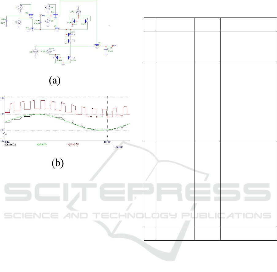
Figure 5: (a) Revised design for the sample and hold circuit
- Utilizing a voltage source approach; (b) Indicated relate
across the circuit’s input and output.
4
CONCLUSION
By doing away with the operational amplifier, the
method presented in this work allows for a more intu-
itive sample and holds execution at much lower power
utilization, with a minimized distortion of 0.037 volts.
Another benefit is the proximity synchronization of
device S1 to the switching device, which successfully
minimizes exaggeration. Additionally, this circuit ef-
fectively circumvents the problem of DIBL (drain-
induced barrier lowering).
ACKNOWLEDGEMENTS
This work has been completed in the Central Labo-
ratory of Computer Science and Engineering depart-
ment of the University of Engineering and Manage-
ment, Jaipur, Rajasthan, India.
Table 1: Table of Performance Evaluation.
Sl
No
Circui
t
Type
Distortion
(V)
Explanation
1 Conventional 0.209 Issues of cloc
k
Feed
through and NMOS
resistance effects
lead to sampling
errors.
2 Bootstrap 0.042
The duty cycle and
ON time are
controlled because
the charge of the
bootstrap capacitor
must be refreshed. In
addition, Input
through the threshold
affects the channel
charge and switch
resistance (S0).
3 Propose
d
0.036
Transistor S1
operates in the region
of inversion while
switch S0
b
ehaves in
the triode region.
Due to this
difference, there
might be differen
t
threshold voltages,
p
otentially leading to
some circuit
inaccuracies.
4 Revise
d
0.029 Diminishe
d
Distortion Effect
REFERENCES
D, P. K. and Beulet, P. A. S. (2018). Design of sample and
hold for high-speed analog to digital converter. VLSI
Design: Circuits, Systems and Applications: Select
Proceedings of ICNETS2, V.
Gupta, Ritesh, and Gamad, R. S. (2022). Sample and hold
circuit design using double sampling without op amp.
NeuroQuantology, 20(14):1422.
Heußen, Sascha, Postler, L., Rispler, M., Pogorelov,
I., Marciniak, C. D., Monza, T., Schindler, P., and
Mu¨ller, M. (2023). Strategies for a practical
advantage of fault-tolerant circuit design in noisy
trapped-ion quantum computers. Physical Review A,
107(4):042422.
Huang, Chi-Wei, Lai, C.-K., Hung, C.-C., Wu, C.-Y.,
and Ker, M.-D. (2023). A cmos synchronized sample-
and-hold artifact blanking analog front-end local field
potential acquisition unit with ±3.6-v stim- ulation
artifact tolerance and monopolar electrode- tissue
IC3Com 2024 - International Conference on Cognitive & Cloud Computing
88

impedance measurement circuit for closed-loop deep
brain stimulation socs. IEEE Transactions on Circuits
and Systems I.
Iizuka, Tetsuya, Ito, T., and Abidi, A. A. (2018). Com-
prehensive analysis of distortion in the passive fet
sample-and-hold circuit. IEEE Transactions on Cir-
cuits and Systems, 65(4):1157–1173–218.
Kim, Jinwoo, Yoon, D., and Cho, Y. (2019). Active
gate control method for voltage balancing of series-
connected sic mosfets. IEEE 4th International Future
Energy Electronics Conference (IFEEC), pages 1–5.
Li, Shuowei, Ojima, N., Xu, Z., and Iizuka, T. (2022). Anal-
ysis and simulation of mosfet-based gate-voltage-
independent capacitor. Photonics and Nanostructures -
Fundamentals and Applications, 61:064501.
P., A. V. and Jacob, J. (2022). Design of sample and hold
circuit with improved charge leakage and linearity for
low power applications. 19th INDICON, pages 1–6.
Velagaleti, SilpaKesav, Nayanathara, K. S., and Madhavi,
B. K. (2019). A sample and hold with clock booster
for improved linearity. 6th International Confer- ence
on Signal Processing and Integrated Networks (SPIN),
pages 1058–1062.
Optimized Sample and Hold Design Leveraging MOSFETs Using SPICE Simulation
89
