
Logic Locking for Random Forests: Securing HDL Design and FPGA
Accelerator Implementation
Rupesh Raj Karn, Johann Knechtel and Ozgur Sinanoglu
Center for Cyber Security, New York University, Abu Dhabi, U.A.E.
Keywords:
Logic Locking, XOR/XNOR Gates, Decision Tree, Random Forest, FPGA, Sklearn.
Abstract:
Logic locking has garnered significant attention due to its promising role in safeguarding intellectual property
against potent threats across the integrated circuit supply chain. The locking mechanism introduces additional
logic elements, so-called key-gates into a circuit, effectively securing the original design with a confidential key.
This work utilizes locking to secure the hardware design of random-forest (RF) machine learning models. With
the correct key, the design produces accurate inference outcomes; otherwise, it generates incorrect inferences.
We explore field-programmable gate array (FPGA) implementation options to realize such locked inference
accelerators. We propose an end-to-end methodology, spanning from the high-level RF hardware design,
locking of those designs, to the FPGA implementation and performance evaluation. Our study employs Intel’s
DE-10 standard FPGA, and we utilize multiple real-world datasets to illustrate the effectiveness of our approach.
1 INTRODUCTION
Over the last decade, significant progress has been
achieved in the design and assessment of logic lock-
ing, a leading method for ensuring the integrity of
integrated circuits across the electronics supply chain
(Sisejkovic et al., 2021). Logic locking manipulates a
hardware design by linking the right functionality to a
secret key known only to the legal intellectual property
(IP) owner (Yasin et al., 2020). The applicability, fea-
sibility, and effectiveness of logic locking have been
thoroughly investigated, with research interests includ-
ing metrics that evaluate the consequences of locking
at multiple levels of abstraction, threat modeling, at-
tack resiliency, etc. (Gandhi et al., 2023).
Hardware implementations of machine learning
(ML) models, particularly on field-programmable gate
arrays (FPGAs), offer significant performance advan-
tages but are susceptible to several attacks and IP
theft (Provelengios et al., 2019). Logic locking tech-
niques address this vulnerability by introducing ob-
fuscation mechanisms that can lock the underlying
design while preserving its functionality. Additionally,
with locking, developers can safeguard proprietary
algorithms, prevent unauthorized access to sensitive
data, and maintain the trustworthiness of ML-driven
systems deployed in real-world environments. When
securing the hardware designs of ML applications, it is
crucial to minimize the hardware overhead caused by
locking. This is especially important because ML oper-
ations often occur on hardware with limited resources,
aiming to accelerate inference.
This article demonstrates how to protect supervised
ML inference on FPGAs using a combination of ran-
dom forest (RF) and logic locking techniques. Our
notion of the model’s privacy is “the certainty that a
hostile party will not be able to steal the parameters of
the RF model.” Since ML models constitute significant
products and intellectual property for many companies,
the risk of their parameters being stolen is consider-
able. The use of an FPGA allows us to provide a se-
cure, accelerated computing platform where hardware-
efficient locking protocols can be implemented.
In summary, our contributions are as follows:
1.
A logic locking technique is devised to protect the
hardware design of RFs.
2.
The behavioral level of abstraction for RFs is sim-
ulated, and logic locking is directly applied to
the hardware-description-language (HDL) source
code.
3.
An FPGA implementation of the locked RFs is
assessed across various datasets on an Intel FPGA.
The source code to reproduce the results of the paper is
available at https://github.com/rkarn/Locking-DT-RF.
Karn, R. R., Knechtel, J. and Sinanoglu, O.
Logic Locking for Random Forests: Securing HDL Design and FPGA Accelerator Implementation.
DOI: 10.5220/0013108000003899
In Proceedings of the 11th International Conference on Information Systems Security and Privacy (ICISSP 2025) - Volume 2, pages 463-473
ISBN: 978-989-758-735-1; ISSN: 2184-4356
Copyright © 2025 by Paper published under CC license (CC BY-NC-ND 4.0)
463

2 PRELIMINARIES
2.1 Random Forests
Consider a trained RF model with decision trees
(DTs). Within these trees, there are N internal nodes
denoted as
I
1
,I
2
,...,I
N
, and n terminal or leaf nodes
denoted as
T
1
,T
2
,...,T
n
. Now, assume a training
dataset
= [
x
,
y
]
, where
x
represents the train-
ing samples, and
y
represents the class labels. In the
context of classification, each leaf node is associated
with one of the class labels from
y
. Also, consider
L
features in the dataset and
x
i
,
1 ≤ i ≤ L
, represents
the
i
-th feature. The number of unique values in
y
corresponds to the number of class labels ℓ.
Each internal node
I
k
in a tree employs a decision
rule based on a threshold value
Λ
k
. This rule relies on
the data feature
x
k
at node
I
k
and the threshold value
Λ
k
. This inequality is used in the rule of node
I
k
and
can be expressed as:
x
k
< Λ
k
or
x
k
≥ Λ
k
(1)
The architecture of an RF model can be expressed
as
( )
. Then,
M
j
(
N
j
,
n
j
) ∈
for
1 ≤ j ≤
, where
the indices
j
correspond to each DT out of the total of
trees. The notation
(
N
j
,
n
j
)
signifies the counts of
internal nodes and leaves in the j
th
DT.
RF inference entails the traversal of each DT, start-
ing from the root node and concluding at one of the
leaf nodes. The internal nodes encountered during this
traversal are determined by a series of inequalities re-
sembling those described in Equation 1. The inferred
label is associated with the leaf node reached at the
end of this traversal; specifically, it is one of the class
labels denoted as
b
j
∈ [0, ℓ − 1]
from the dataset for
the
j
th
DT. The ultimate prediction is derived through
a majority voting process, where the predictions of
each DT are collectively considered:
b = majority voting(b
1
,b
2
,....,b
j
,b
j+1
,...,b ) (2)
2.2 Locking at Behavioral Level
Logic locking can be implemented for various stages
of the design process, namely at system level, register-
transfer level (RTL), netlist/gate level, and transistor
level, each offering its own set of advantages and con-
siderations. While a comprehensive study of locking
across these stages is beyond the scope of this work,
we provide a generic comparison of behavioral and
netlist/gate-level locking in Table 1, as netlist/gate-
level locking is prominently utilized in the literature.
We argue that deploying logic locking at the be-
havioral level, which is a higher abstraction than RTL,
provides designers with the flexibility to analyze vari-
ous aspects related to high-level performance and se-
curity characteristics. Additionally, our methodology
could serve as a benchmarking framework for the ML
community to conduct exploratory experiments before
transitioning to netlist/gate-level implementations.
2.3 Random Logic Locking
Without loss of generality, here we apply random
logic locking (RLL) to secure the design of RF mod-
els. RLL is a hardware security technique utilized
to safeguard integrated circuits (ICs) from reverse
engineering and unauthorized access (Yasin et al.,
2019). In this method, additional logic gates, par-
ticularly XOR/XNOR gates, are integrated at random
locations into the IC’s design. The activation or “un-
locking” process involves feeding the secret key to
these XOR/XNOR gates, altering the circuit’s func-
tionality based on the key’s binary values – only the
correct key will ensure the correct circuit functionality.
While RLL offers some promises, it remains vul-
nerable to analytical attacks based on Boolean sat-
isfiability (SAT) (El Massad et al., 2019) and ML
techniques (Alrahis et al., 2021).
1
To mitigate this,
researchers have proposed various countermeasures
and improvements to RLL:
1.
Complexity (Xie and Srivastava, 2018): Increasing
the complexity of the random logic inserted into
the design can make SAT attacks more difficult by
creating a larger search space.
2.
Key Whitening (Bhatia and Som, 2016): Combin-
ing the original secret key with a randomly gener-
ated value through cryptographic operations. This
technique can improve the randomness and unpre-
dictability of the secret key, making it harder for
attackers to guess or infer.
3.
Diversification (Yasin et al., 2017): Using mul-
tiple, different locking techniques or combining
RLL with other security measures can increase the
difficulty for attackers.
Although these techniques have not been integrated
into our work at present, they are directly relevant to
our objectives. We plan to consider them in future
work, whereas our current focus lies in prototyping
the idea of locking RFs. More detailed discussions on
such security aspects are given in Section 4 and 6.1.
1
SAT attacks entail framing the problem of unlocking the IC’s
functionality as a Boolean satisfiability problem, where attackers
iteratively seek for input assignments that rule out incorrect key can-
didates. ML attacks learn the correlation between the locked IC’s
observable structure and/or behavior and its hidden original func-
tionality by training models on locked ICs, subsequently predicting
the hidden functionality of other locked ICs.
ICISSP 2025 - 11th International Conference on Information Systems Security and Privacy
464
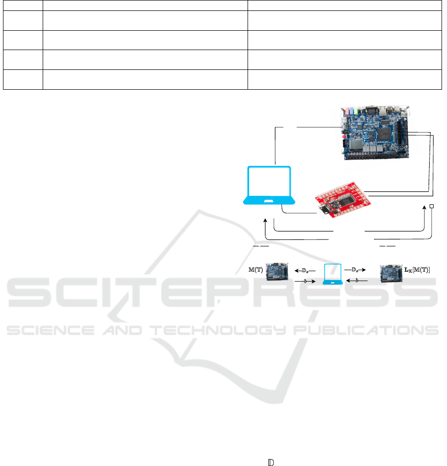
Table 1: Comparison of logic locking at behavioral level vs. netlist level.
Aspect Logic Locking at Behavioral Level Logic Locking at Netlist Level
Stage
Implemented at an early stage of the design (before gate-level synthesis)
(Sisejkovic et al., 2021).
Applied after the design has been synthesized into gate-level netlist
(Sisejkovic et al., 2021).
Complexity Low, since it focus on high-level abstractions and functional descriptions
(Pilato et al., 2021).
Potentially more complex because netlist level involves low-level
gate and flip-flop structures (Pilato et al., 2021).
Security
May provide a lower level of security as it is applied earlier in the design
flow, allowing more opportunities for analysis (Almeida et al., 2023).
Often more secure as it is applied later, making it harder for attackers
to analyze and reverse-engineer the design (Almeida et al., 2023).
Overhead
Typically less likely to introduce significant performance overhead (En-
gels et al., 2022).
A greater performance impact due to modifications at the gate-level
(Engels et al., 2022).
2.4 Logic Locking vs Data Encryption
One question frequently raised regarding the use of
logic locking is, “Could we just encrypt the actual
data/outputs instead of locking the internal circuitry?”
While encryption is indeed a viable approach for
data protection, locking has several advantages. First,
locking ensures that the actual IP of the circuit design
remains protected, not only the processed data. Sec-
ond, locking the circuitry itself makes it harder for
adversaries to clone the design by reproducing some
observed output data. That is, even if attackers could
replicate some outputs for some cases, without knowl-
edge of the internal architecture, the cloned design
would very likely lack in functionality and exhibit dif-
ferent behavior for other data inputs. Lastly, logic
locking typically allows for more customization than
regular ciphers, thereby helping to meet different de-
sign requirements and security goals.
3 METHODOLOGY
In our workflow (Fig. 1), we utilize the open-source
Python library sklearn for training of RF models. Once
the training phase was completed, we extracted all the
decision rules from the root node to each leaf node.
Subsequently, these rules were translated into Verilog
source code, along with locking. To facilitate this
transformation, we employed an algorithm as in (Karn
et al., 2023). Logic locking is subsequently applied to
these decision rules. In the remainder of this section,
we provide more implementation details.
3.1 Circuit Design, Runtime Operation
We implement RFs using a sequential-circuit design
approach as outlined in (Karn, Rupesh Raj and Nawaz,
Kashif and Elfadel, Ibrahim Abe M, 2023). In such
designs, each DT is treated as a finite state machine
(FSM), where the transition diagram of the FSM mir-
rors the branching structure of the DT, and each node
in the DT corresponds to a unique FSM state. Thus,
Host machine
Quartus
Verilog
Expt. 1 Expt. 2
Plain Random
Forest model
Locked Random
Forest model
Python Sklearn
DE-10 Standard FPGA
inference data
inferred class or label
Client-A (Alice)
Client-B (Bob)
Client-A (Alice)
USB Cable
FT232RL
UART Connection
GPIO[0]
TxD
RxD
GPIO[1]
sof file
USB 2.0
USB-A
Figure 1: Methodology workflow and runtime operation.
the total number of nodes in each DT matches the num-
ber of FSM states. To maintain and update these states,
flip-flops are utilized, and they are synchronized by a
common clock signal.
The FSM representation of a DT is illustrated in
Fig. 2, where each state
i
is denoted as S
i
. In ev-
ery clock cycle, one of the FSM states is assessed by
checking a specific inequality relation, as expressed
in Equation 1. In the hardware implementation, this
evaluation is accomplished using a comparator and a
multiplexer, as depicted in Fig. 2 as well. The enti-
ties required for the comparison, i.e. the individual
features
x
i
and the threshold values
Λ
j
′
s
, are directly
annotated in the behavioral description of the FSM.
Initially, all data samples for inference are
streamed through the input ports of the FPGA and
being stored in the BRAM. As per the behavioral de-
scription, at runtime, the feature values from the infer-
ence samples are retrieved from the BRAM and fed
into the root node of the DT, specifically into the ini-
tial FSM state
S
1
. In the subsequent clock cycle, the
following state, either S
2
or S
3
, is determined based
on the result of the inquiry made during the previous
state. This sequential process continues until it leads
to a leaf, which signifies a terminal node
T
i
. Once this
Logic Locking for Random Forests: Securing HDL Design and FPGA Accelerator Implementation
465
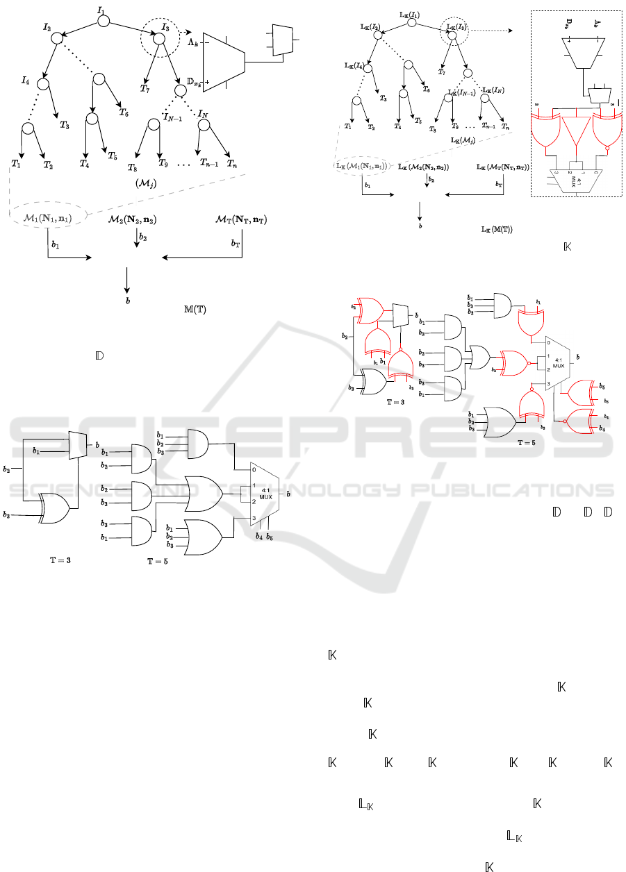
Fig: Architecture of a decision tree in random forest.
............
Majority Voting
RF final outcome
Fig: Architecture of a random forest .
V
cc
Gnd
Comparator
0
1
S0
Mux
1
0
S
1
S
2
S
4
S
N-1
S
N
State of FSM : S
i
S
3
Figure 2: Within the context of an RF, DTs operate as fol-
lows: At every node, a comparison is made between a dataset
feature denoted as
x
k
and a given threshold represented as
Λ
k
. If the result of this comparison is true, the left branch of
the node is evaluated; otherwise, the right branch is assessed.
The lower part illustrates the outcome of each DT during the
inference process in the RF.
0
1
S0
Mux
Figure 3: Majority voting over each DT’s outcome (
b
j
’s),
to obtain the final inference outcome of the RF model (
b
).
Derived from (Choudhary et al., 2019).
leaf is reached, the class or label associated with
T
i
is
returned as the result of that particular DT. The same
process is applied to all other trees of the RF model.
Next, after obtaining the inference results from all
DTs, the FSM is reset, and the logic transitions into
the majority-voting mode. The diagram depicting this
process for two architecture (different number of DTs
in the RF) is given in Fig. 3. Subsequently, when the
final inference result
b
is computed via Equation 2, the
system is reset and remains in standby mode until a
new inference request is received.
3.2 Locking the RF: Procedure
In general, the locked design of an RF model’s acceler-
ators ensures accurate inference outcomes only when
Fig: Architecture of a locked decision tree in random forest.
............
Locked Majority
Voting
RF final outcome
Fig: Architecture of a locked random forest
.
S
1
S
2
S
4
S
N-1
S
3
S
N
State of FSM : S
i
Random
Selection
XNOR key
gate
V
cc
Gnd
Comparator
0
1
S0
Mux
1
0
𝕜
𝕜
XOR key
gate
Buffer
Figure 4: Locked RF. At each node
i
, the key
(i)
is repli-
cated as shown in node I
3
.
0
1
S0
Mux
𝕜
𝕜
𝕜
𝕜
𝕜
𝕜
𝕜
𝕜
Figure 5: Locked majority voting corresponding to Fig. 4.
The key-gates are highlighted in red.
provided with the correct key. As indicated, the train-
ing process involves utilizing a dataset
= [
x
,
y
]
.
Next, i.e., post-training, RLL is conducted as follows.
XOR/XNOR key-gates are added for random nodes of
the DTs. The choice between XOR and XNOR gates
is also determined by a random process. This random-
ness adds an extra layer of complexity and ambiguity
to the locking mechanism, making it more resistant to
adversarial attacks (Taran et al., 2019). More specifi-
cally, we devise a strategy where the value of the key
comprises a sequence of randomly generated binary
bits. The choice between XOR and XNOR operations
is then determined by the value of the key ; if the
i
-th
bit of is equal to
1
, the corresponding key-gate is
XOR; if it is equal to
0
, the gate becomes XNOR. For
any bit
(i)
, the following condition is always satisfied:
(i)
⊕1 =
¯
(i)
; (
(i)
⊕1)⊕1 =
(i)
;
(i)
⊕0 =
(i)
To illustrate the locking procedure for one of the
trees
(M
1
(N
1
,n
1
))
using the key within the RF,
refer to Fig. 4. The same locking procedure is executed
for the remaining trees, such as
(M
2
(N
2
,n
2
))
, etc.
The locking process for the majority voting is shown
in Fig. 5. Notably, the key is partitioned into two
ICISSP 2025 - 11th International Conference on Information Systems Security and Privacy
466

components, namely and , each serving the pur-
pose of locking individual DTs within the RF and the
majority voting mechanism, respectively.
= [
1
,
2
,...., ] (3)
i
= [
1
,
2
,....,
N
i
]; 1 ≤ i ≤ (4)
= [
b
1
,
b
2
,...,
b
] (5)
In short, key-gates are positioned at the output of
every decision node within the DT or state of the FSM.
Random decisions determine whether to employ an
XOR gate, XNOR gate, or no key-gate (buffer) for
securing the decision node (use of buffers is justified
in Section 6.1). Similarly, for the majority voting, key-
gates are randomly distributed across various locations,
identified in red.
The number of bits
| |
in the key can be esti-
mated, from Equations 3–5, as follows:
| | = ; |
i
| = N
i
| | = | | + | | =
∑
i=1
N
i
+ (6)
3.3 Locking the RF: Implementation
Implementing the DTs of an RF model in Verilog, us-
ing a behavioral-level FSM, involves translating the
logical structure of the trees into a set of states and
transitions within the FSM. As indicated earlier, each
state represents a decision node in the tree, while tran-
sitions between states correspond to the outcomes of
decisions made at each node.
Toward that end, Verilog’s
case
statement is a pow-
erful construct commonly used to model FSMs. By
organizing the case statements appropriately, designers
could model the hierarchical structure of a DT in clear
and concise manner. We adopted a similar strategy and
furthermore insert key-dependent state transitions. As
explained in Section 3.2, the XOR/XNOR key-gates
are randomly selected at a few nodes of each tree in the
RF. The following pseudocode illustrates an example
of such implementation. In fact, this behavioral code
generates the circuit shown in Fig. 4.
Listing 1: State transition logic in Verilog.
c as e ( s t a t e t r e e 1 )
10 ’ d0 : i f ( ( D x t r e e 1 [ 4 0 7 ] <= 0 ) ˆ K t r e e 1 [ 0 ] ) s t a t e t r e e 1 <= 1 ;
e l s e s t a t e t r e e 1 <= 2 3 8;
10 ’ d1 : i f ( ( D x t r e e 1 [ 3 8 6 ] <= 1 2) ˜ ˆ K t r e e 1 [ 1 ] ) s t a t e t r e e 1 <= 2 ;
e l s e s t a t e t r e e 1 <= 1 2 3;
10 ’ d2 : i f ( ( D x t r e e 1 [ 7 1 4 ] <= 0 ) ˆ K t r e e 1 [ 2 ] ) s t a t e t r e e 1 <= 3 ;
e l s e s t a t e t r e e 1 <= 6 6 ;
10 ’ d3 : i f ( ( D x t r e e 1 [ 3 4 6 ] <= 0 ) ˜ ˆ K t r e e 1 [ 3 ] ) s t a t e t r e e 1 <= 4 ;
e l s e s t a t e t r e e 1 <= 3 5 ;
10 ’ d4 : i f ( ( D x t r e e 1 [ 3 5 0 ] <= 0 ) ˜ ˆ K t r e e 1 [ 4 ] ) s t a t e t r e e 1 <= 5 ;
e l s e s t a t e t r e e 1 <= 2 0 ;
10 ’ d5 : i f ( D x t r e e 1 [ 1 5 6 ] <= 1 ) s t a t e t r e e 1 <= 6 ;
e l s e s t a t e t r e e 1 <= 1 3 ;
10 ’ d6 : i f ( ( D x t r e e 1 [ 4 3 0 ] <= 0 ) ˜ ˆ K t r e e 1 [ 6 ] ) s t a t e t r e e 1 <= 7 ;
e l s e s t a t e t r e e 1 <= 1 0 ;
10 ’ d7 : i f ( ( D x t r e e 1 [ 1 7 6 ] <= 3 ) ˜ ˆ K t r e e 1 [ 7 ] )
be g in L a b e l t r e e 1 <= 7 ; s t a t e t r e e 1 <= 0 ; end
e l s e b eg in L a b e l t r e e 1 <= 2 ; s t a t e t r e e 1 <= 0 ; end
10 ’ d8 : i f ( D x t r e e 1 [ 2 1 2 ] <= 2 )
be g in L a b e l t r e e 1 <= 4 ; s t a t e t r e e 1 <= 0 ; end
e l s e b eg in L a b e l t r e e 1 <= 9 ; s t a t e t r e e 1 <= 0 ; end
. . . . . . . .
en dc a se
In our implementation, note that the states
{0,1,2,3,4,5,6}
cover intermediate nodes, while
states
{8,9}
represent nodes expanding to the terminal
nodes or leaves, as the outcome of the inference is
stored in the ‘Label tree1’ register at this state. The
notation ‘D x tree1’ refers to the memory containing
data features
x
, utilized for inferring the first tree of
the RF. Similarly, the variable ‘state tree1’ represents
the next state or state transition register, while
‘K tree1’ symbolizes the key for the first tree. Nodes
{0,1,2,3,4,6,7}
are randomly selected to incorporate
key-gates, which are triggered/operated correctly only
with the right key. The operators ‘ˆ‘ and ‘˜ˆ‘ denote
XOR and XNOR operations, respectively. Again, a
similar approach is applied to lock the majority voting,
as depicted in the circuit diagram in Fig. 5. Note that
the use of ‘ˆ‘ and ‘˜ˆ‘ operators in Listing 1 serves as
a high-level abstraction to represent key-dependent
logic functions. These operators are mapped onto
the FPGA’s LUTs during synthesis, ensuring that
the intended logic locking remains intact in the
synthesized and implemented design.
3.4 FPGA Implementation: Synthesis
for Locked Design
FPGA synthesis is a multi-faceted process. For our
work, the specific aim would be to limit the overhead
introduced by the locking mechanisms. Conventional
optimization techniques use, e.g., logic duplication
to improve timing performance.
2
By carefully tailor-
ing optimization strategies, we aim to strike a balance
between improving synthesis results and preserving
the integrity of the locking mechanisms. Toward that
end, the tool of our choice, Quartus Prime, offers a
configuration of the optimization level, where higher
levels would prioritize classical synthesis metrics –
power, performance, and area – but could inadver-
tently compromise the locking scheme. Lower levels
prioritize preserving the original design structure and
minimizing vulnerabilities, albeit with some resource
overheads. This balance becomes evident in Section 5,
2
While logic duplication may reduce critical path delays and
improve performance, it can also increase resource overhead by
adding redundant logic elements. Moreover, this redundancy might
make the design more vulnerable to attacks. That is, adversaries
could target at exploiting the different copies of the same logic
function – which may not all be locked to the same degree, due to
the randomized procedure for RLL – to gain unauthorized insights.
Logic Locking for Random Forests: Securing HDL Design and FPGA Accelerator Implementation
467

where only marginal overheads arise due to logic lock-
ing, all while maintaining the integrity of the locked
design and providing strong protection especially for
larger, more complex and, thus, more practical/real-
world accelerator designs.
4 THREAT MODEL
The designer is a trusted entity, meaning that both the
personnel and the tools utilized in the creation of the
RF model’s accelerators are acting benign. In this sce-
nario, the attacker has only access to the functional
FPGA containing the pre-loaded bitstream file, but
not the design process. The bitstream was obtained
from the synthesized netlist which was, in turn, gen-
erated from the circuit representing the RF locked at
the behavioral level, as explained in Section 3.2. The
attacker possesses knowledge of the logic locking al-
gorithm employed. The sole part concealed from the
attacker is the secret key value , which takes the form
of a binary vector.
Adversaries targeting this notion of logic locking of
RF accelerators may employ various strategies, such as
model extraction, reverse engineering, exploiting side-
channels, or identifying vulnerabilities within the logic
locking mechanisms themselves. Their objectives may
include accessing node’s threshold values and decision
transition from the locked model, undermining the
decision-making processes, or gaining an unauthorized
competitive advantage.
Countermeasures against such attacks may include
the strategies outlined in Section 2.3 to, e.g., defend
against SAT and ML-based attacks. Further, the coun-
termeasures could involve implementing robust intru-
sion detection systems, managing side-channel infor-
mation leakage, and continuously monitoring for mali-
cious behavior. Our assumption is that such measures
are implemented after the deployment of the locked RF
accelerators on the FPGA. This is because our primary
focus in this paper is on evaluating the locking mech-
anism and its associated performance impact across
different datasets on the FPGA. Note that, a straightfor-
ward first line of defense would be to employ bitstream
encoding, thereby preventing naive reverse engineer-
ing and model extraction attacks.
5 EXPERIMENTAL EVALUATION
5.1 Setup
Synthesis of the Verilog source code for the locked RF
was carried out using the Quartus Prime Design Suite.
Table 2: DT’s architecture (nodes, leaves) in the RF model
and accuracy with
= 3
. For the DT experimentation, the
first tree M
1
(N
1
,n
1
) is used.
Dataset Architecture Accuracy (%)
(N
1
,n
1
) (N
2
,n
2
) (N
3
,n
3
) Train Test
MNIST (485, 243) (493, 247) (501, 251) 85.53 85.12
Accdel (483, 242) (471, 236) (475, 238) 62.94 61.63
Activities (215, 108) (189, 95) (223, 112) 93.07 92.48
Wearable (389, 195) (413, 207) (517, 259) 91.46 90.81
Wireless (441, 221) (489, 245) (395, 198) 98.46 98.17
For the FPGA implementation, we selected the DE-10
Standard SCSXFC6D6F31CN FPGA board (de1, ).
3
Without loss of generality, the FPGA clock frequency
is set to
50MHz
. The FPGA is connected to a host
machine through USB port.
Two inference experiments, denoted as Expt1 and
Expt2, were conducted. In Expt1, the RF model was
implemented on the FPGA without any form of lock-
ing, while in Expt2, the RF was locked as detailed in
Section 3. Out of all the nodes in the DT,
85%
were
randomly selected for locking, whereas the remaining
nodes were assigned as buffers. For both experiments,
we employ the widely recognized MNIST dataset (Le-
Cun et al., 1998), which consists of grayscale images
of handwritten digits ranging from
0
to
9
, i.e., 10
classes are considered. The dataset’s features are based
on the grayscale image’s pixel values, with a size of
L = 28 × 28 = 784
. Furthermore, our analysis extends
to four other datasets, namely Accdel (Dua and Graff,
2017), Activities (Ugulino et al., 2013), Wearable (Vel-
loso et al., 2013), and Wireless (Torres et al., 2013).
4
5.2 Results: Inference Accuracy
We report the inference accuracy on various DT archi-
tectures in Table 2. Both the locked and unlocked de-
signs exhibit identical accuracy, confirming that there
is no performance degradation due to locking.
To further improve accuracy for some datasets, a
comprehensive hyper-parameter tuning process would
be recommended, involving parameters like nodes,
leaf, depth, randomness, entropy, and the number of
trees. While we acknowledge the significance of such
tuning process, it is essential to note that our primary
objective is not to enhance the training and testing
accuracy of different RF architectures, but rather to
3
That FPGA has a total of
41,910
adaptive logic modules
(ALMs),
4,191
logic array blocks (LABs),
83,820
flip-flops (FFs),
499
input-output (IO) pins,
1,12
digital signal processing (DSP)
modules, and 5,53 block RAMs (BRAMs) each of 10Kb.
4
Accdel is a dataset for predicting activities of daily living and
contains 4 features and 14 output classes; Activities is a dataset
for classifying body movements and consists of 18 features and 5
classes; Wearable is a dataset for monitoring weight lifting exercises
and comprises 54 features and 5 classes; Wireless is a dataset for
activity recognition with 8 features and 5 classes.
ICISSP 2025 - 11th International Conference on Information Systems Security and Privacy
468

Table 3: FPGA resource comparison for an RF/DT accelerator with
= 1
. ALUTs: Combinational adaptive look-up tables,
FFs: Primary registers,
F
out
: Max fanout,
F
max
: Max attainable clock frequency, Setup: Slack time for clock setup, Hold: Slack
time for clock hold.
Attributes Unlocked (Fig. 1 Expt1) Locked as per Section 3.2 (Fig. 1 Expt2)
MNIST Accdel Activities Wearable Wireless MNIST Accdel Activities Wearable Wireless
ALMs 953 117 174 331 191 953 116 179 329 194
LABs 154 23 31 55 32 154 19 29 58 28
ALUTs 1257 199 267 410 315 1257 196 265 413 316
FFs 1641 191 309 601 270 1641 191 308 603 266
Max. F
out
1640 189 307 599 268 1640 189 306 601 264
F
max
(MHz) 110.88 173.04 171.32 153.52 152.32 110.88 201.78 168.98 144.24 163.48
Setup (ns) 10.981 14.221 14.163 13.486 13.435 10.981 15.044 14.082 13.067 13.883
Hold (ns) 0.372 0.371 0.370 0.370 0.369 0.372 0.370 0.370 0.372 0.373
Table 4: FPGA resource comparison for an RF accelerator with = 3.
Attributes Unlocked (Fig. 1 Expt1) Locked as per Section 3.2 (Fig. 1 Expt2)
MNIST Accdel Activities Wearable Wireless MNIST Accdel Activities Wearable Wireless
ALMs 1940 140 194 570 373 1940 141 198 667 375
LABs 291 23 36 92 49 291 23 40 101 59
ALUTs 3006 242 292 790 583 3006 239 288 965 580
FFs 3349 240 342 639 488 3349 231 350 644 483
Max. F
out
3348 238 340 637 486 3348 229 348 642 481
F
max
(MHz) 109.18 179.69 169.23 124.6 127.34 109.18 196.5 152.25 102.92 122.55
Setup (ns) 10.841 14.435 14.091 11.974 12.147 10.841 14.911 13.432 10.284 11.840
Hold (ns) 0.249 0.332 0.370 0.369 0.352 0.249 0.362 0.370 0.359 0.361
demonstrate the application of logic locking on an
already trained model.
5.3 Results: FPGA Resources
A study of FPGA resources for a simple DT archi-
tecture versus an RF architecture is given in Table 3
versus Table 4. As expected, the resources consumed
by the locked RF/DT models are larger than those of
the unprotected ones.
Recall that, in Table 1, we hypothesized that lock-
ing at the behavioral level would induce only marginal
overheads. Tables 3 and 4 confirm this. Notably,
the synthesis-related efforts for resource optimization,
as outlined in Section 3.4, help to strategically re-
distribute resource utilization across various FPGA
resources. Furthermore, both setup and hold slacks
remain in the positive range, i.e., the design’s function-
ality and performance is maintained.
MNIST. Resource utilization for both DT and RF
architectures is consistent across the unlocked and
locked designs. Thus, the overhead from the lock-
ing process is negligible when contrasted with the
resources already used by the baseline RF/DT circuit.
Accdel. For the DT architecture, the locked design
demonstrates more resource efficiency compared to the
unlocked one, albeit with a slight hold-time penalty.
Similarly, the locked RF designs exhibits better re-
source efficiency than the unlocked RF design, with
the negligible overhead of one additional ALM.
Activities. The locked DT design consumes more
ALMs and exhibits reduced timing bandwidth com-
pared to the unlocked DT one. In the case of RF,
similarly, the locked design consumes more resources
and offers lower timing bandwidth compared to the
unlocked configuration, except for ALUTs.
Wearable. The locked DT design consumes more
resources and exhibits reduced timing bandwidth com-
pared to the unlocked one, except for ALMs and hold
time. For the RF architecture, the locked configura-
tion shows higher resource consumption in all aspects
compared to the unlocked design. This pattern also
extends to timing bandwidth.
Wireless. For the DT architecture, the locked con-
figuration requires slightly more ALMs, ALUTs, and
larger fan-outs, but also provides superior timing band-
width compared to the unlocked configuration. For
the RF architecture, the locked design consumes more
ALMs and LABs than the unlocked design, with a
benefit gained for hold-time slacks.
Summary. We have successfully verified that the
integrity of the locking structure is maintained. In
summary, locking incurs some overheads, as expected.
Still, these overheads are often marginal and also scale
well for larger and more complex accelerator designs.
Finally, for more challenging scenarios, e.g., aris-
ing for deeper trees as discussed in Section 6.2, timing
optimization and/or pipelining could be applied.
Logic Locking for Random Forests: Securing HDL Design and FPGA Accelerator Implementation
469
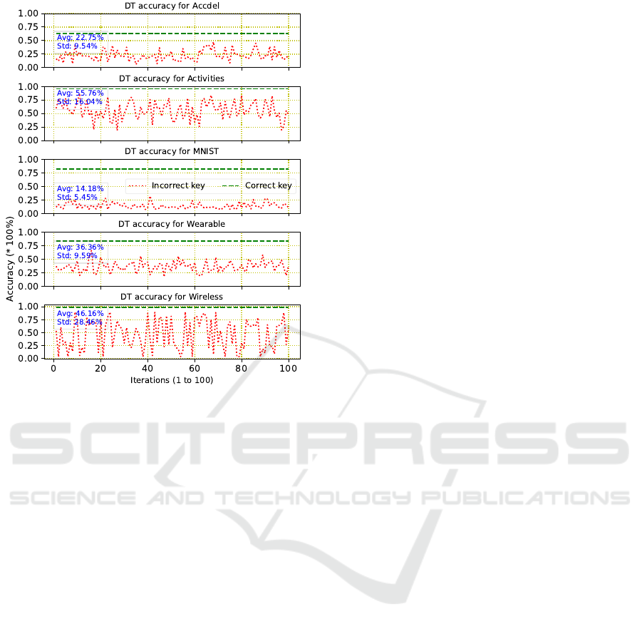
Figure 6: Accuracy comparison of a DT model operated with
the correct key versus randomly generated wrong keys. The
accuracy with the correct key (
−−
) matches the unlocked
accuracy presented in Table 2.
5.4 Results: Key-Guessing Attack
Here, we evaluate the impact of a naive attack that em-
ploys random key-guessing. We compute the accuracy
of a locked DT model while utilizing 100 different,
randomly generated keys. We then compare these ac-
curacy results against the same locked DT model while
utilizing the correct key. The results are visualized in
Fig. 6 and discussed next.
First, it is important to note that we did not employ
any iterative heuristics, i.e., no prior information like
cross-validation of accuracy was used throughout the
100 iterations for the random key-guessing procedure.
Second, it is also important to note that, given that the
correct key is also generated randomly, we can expect
an average Hamming distance of 50% between the
correct and any incorrect key. In other words, even
for a randomly guessed key, we would not expect a
catastrophic drop in accuracy for the locked DT archi-
tecture, or any other locked ML model for that matter.
Third, across the different scenarios/datasets, we do
observe notable differences. More specifically, the
average drop in accuracy is
70.94
percentage points
(pps) for MNIST,
38.88
pps for Accdel,
36.72
pps for
Activities,
54.45
pps for Wearable, and
52.01
pps for
Wireless. Furthermore, the standard deviation for the
reduced accuracy across all 100 random keys is
5.45%
for MNIST,
9.54%
for Accdel,
16.04%
for Activities,
9.59% for Wearable, and 28.46% for Wireless.
These numbers suggest two take-aways as follows.
For one, for the more complex MNIST accelerator,
the proposed scheme works out best: the average drop
in accuracy for random key-guessing is the largest,
whereas the standard deviation for the accuracy ob-
tained across 100 randomly guessed keys is the small-
est. In other words, the impact of random guessing
is most limited and attackers have the lowest chance
to randomly guess a “good” key. This clearly con-
firms the good scalability of the security promises.
For another, with less complex datasets like Activities
and Wireless, the variation of the accuracy across ran-
dom key-guessing is considerable. This means that,
by random chance, attackers can obtain a relatively
“good” key that allows the accelerator to work with
only slightly reduced accuracy. This suggests that ei-
ther the DT model parameters or the model itself are
not robust against such an attack, which is presumably
due to the small number of classes and features for
those cases (Section 5.1). This clearly re-confirms that
the proposed protection scheme scales better for larger
and more complex accelerator designs, which is essen-
tial for real-world application of locking. This also
underscores the need for repeated random sampling of
nodes to be selected for locking, in order to maintain
maximum corruption for any incorrect key.
6 DISCUSSION
6.1 Attacks and Defenses
Attacking a locked DT/RF model on an FPGA can in-
volve various scenarios, each exploiting different vul-
nerabilities and posing unique challenges for defense
efforts. Next, we outline some important scenarios.
Brute-Force Attack. An attacker attempts to gain
unauthorized access by systematically trying different
combinations of keys. We have shown such attack and
its scale in Section 5.4.
Side-Channel Attacks. This scenario is based on ex-
ploiting information leaked during system operation,
such as power or timing patterns, to deduce the lock-
ing key. Such attacks could be particularly promising
against our scheme, as (by random decision) not all
DT nodes will have additional key-gates. Thus, the
power consumption and delays for nodes with key-
gates would be, on average, higher than for the rest
of the nodes (e.g., nodes
{5,8}
in Listing 1 in Sec-
tion 3.3). To thwart such attacks, buffers can be ap-
pended to those nodes without key-gates, seeking to
ICISSP 2025 - 11th International Conference on Information Systems Security and Privacy
470

bring power consumption and delays to the same level
across all nodes.
Man-in-the-Middle (MitM) Attack. Intercepting
communication between the user and the FPGA could
allow an attacker to eavesdrop on or manipulate the
data exchanged during inference. Such attacks fall out-
side the scope of this paper; defending against those
would require orthogonal measures, like network secu-
rity and physical access restrictions.
Fault-Injection Attacks. Inducing faults or errors
during the operation of the FPGA could manipulate
the model’s behavior or compromise the integrity of
the computations. Similar to MitM attacks, this type
of attack falls outside the scope of this paper. This is
also because it requires somewhat more sophisticated
equipment and know-how for attackers, as it relies
on exploiting the fabric utilized in building the FPGA
chip and peripherals. For defenses, one could consider
tamper-proof memories, phase-locked loops (to detect
clock glitches), monitoring of I/O buses, etc.
Denial-of-Service (DoS) Attacks. Overloading the
FPGA with malicious traffic or requests could disrupt
the availability of the RF model. Defenses would re-
quire efficient access control mechanisms, e.g., based
on fair-share policies. Furthermore, access manage-
ment requires error detection and correction mecha-
nisms to mitigate the impact of maliciously crafted
inputs. Additional techniques such as employing re-
dundancy of the RF model and failover mechanisms
can help maintain the overall system availability in
case of such attacks.
Reverse-Engineering Attacks. Analyzing the bit-
stream or the physical layout of the FPGA to deduce
details of the RF design could potentially reveal sen-
sitive intellectual property. Similar to fault injection,
such attacks may require more expertise to exploit the
FPGA fabric’s physical layout. Also recall that bit-
stream encryption can be applied as simple first line
of defense against such attacks.
6.2 Scaling Trees
As the demand for deploying ML models on FPGAs
continues to rise, addressing the scalability challenges
of logic locking in DTs and RFs becomes imperative
when deploying on resource-constrained FPGAs. Par-
ticularly, when dealing with dense trees (large
{
N
i
,
n
i
}
)
or a large number of trees for the majority voter,
some parts of the proposed methodology may need to
be re-visited as follows.
Dense Trees. In scenarios where DTs become ex-
cessively dense (large
{
N
i
,
n
i
}
), the overhead associ-
ated with inserting key-gates can increase substantially.
This can lead to resource constraints on the FPGA, ul-
timately impacting scalability.
The average complexity
C
of logic locking for an
RF model’s implementation on an FPGA can be ex-
pressed (with big ‘O’ notation) as the sum of complex-
ities for each DT:
C
RF
= O
×
N
i
∑
i=1
(n
i
× L ×
i
)
!
(7)
This equation captures the average overhead associated
with inserting key-gates at each node in every DT. To
mitigate this challenge, techniques such as estimating
a node’s importance and segmenting the nodes into
important and less-important could be employed. Here,
less-important nodes are those that impact minimally
on the inference performance if such nodes were to be
removed from the tree.
Note that, in sklearn, the framework of our choice
for this work, DTs do not inherently assign such as-
sessment to individual nodes. Nevertheless, the sig-
nificance of features can be gauged via the concept
of Gini impurity, which then indirectly reflects on the
nodes’ importance. More specifically, features con-
tributing to substantial reductions in impurity at nodes
are deemed more significant. Typically, within DTs,
nodes closer to the root tend to hold greater importance.
Accordingly, we propose the following steps.
▷
Node Importance Estimation: We define the impor-
tance
i
of each node
i
based on its impact on the
overall inference performance. One approach is
to calculate the Gini impurity
i
at each node and
define
i
inversely proportional to
i
, i.e.,
i
∝
1
i
.
▷
Key-Gate Allocation (KGA): We allocate key-gates
selectively to nodes based on their importance
i
and their proximity to the root. Let
θ
denote a
threshold for node importance. More specifically,
we allocate key-gates as follows:
KGA =
Add key-gates to node i if
i
≥ θ
Assign buffer if
i
< θ
(8)
Nodes with importance
i
exceeding the threshold
θ
are considered significant and receive key-gates,
while less important nodes are assigned buffers.
▷
Memory-Map Optimization: To optimize FPGA
resource utilization, we utilize techniques such as
memory-map optimization. By efficiently orga-
nizing memory access patterns, we can reduce re-
source overhead and improve overall performance.
Many Trees. Likewise, when dealing with RFs con-
taining numerous trees used for majority voting,
concerns regarding scalability emerge due to the com-
pounding impact of locking multiple DTs. Each ad-
ditional DT introduces intricacy to the overall locked
Logic Locking for Random Forests: Securing HDL Design and FPGA Accelerator Implementation
471

circuit, potentially straining the FPGA resources. Tack-
ling the scalability challenges inherent in large RFs
necessitates employing the following strategies:
▷
Tree Pruning: Through the selective removal of
redundant or less informative branches, tree prun-
ing optimizes the balance between model accu-
racy and computational efficiency. The number of
nodes and leaves (N
i
′
, n
i
′
) after pruning is less than
N
i
and n
i
, respectively. Thus, from Equation 7,
the complexity is reduced. Pruning facilitates the
seamless integration of locking mechanisms by
reducing the complexity of individual DTs.
▷
Ensemble-Based Optimization: Within ensemble
optimization, trees that consistently under-perform
during the ensemble process can be identified and
omitted from the ensemble to conserve FPGA
resources for the more effective trees and en-
hance their locking capabilities. Let
′
represent
the optimized number of trees. The complexity
C
ensemble+pruning
after optimization and pruning to-
gether can be expressed as:
C
ensemble+pruning
= O
′
×
N
i
′
∑
i=1
(n
i
′
× L ×
i
′
)
!
(9)
With ensemble optimization and pruning, the com-
putational complexity C
ensemble+pruning
< C
RF
.
▷
Parallelization: By dispersing locked RF in-
ference tasks across multiple processing units
or FPGA slices, parallelization maximizes re-
source utilization and minimizes processing bot-
tlenecks. Let denote the number of parallel
processing units. The computational complexity
C
ensemble+pruning+parallel
with parallelization along
with ensemble and pruning can be expressed as:
C
ensemble+pruning+parallel
=
C
RF
(10)
It is evident that
C
ensemble+pruning+parallel
<<< C
RF
.
This simultaneous execution of locked inference
operations expedites the overall inference process.
6.3 Adaptation to Other ML Models
The proposed logic locking mechanism, while demon-
strated on DTs and RFs, is inherently adaptable to a
wide range of ML models. This adaptability stems
from the fundamental principle of inserting key-gates
into the hardware representation of the model, which
is independent of the specific algorithmic structure of
the model. For instance, in neural networks, key-gates
can be introduced at various points, such as between
layers or within the activation functions, ensuring that
only the correct key allows for accurate forward prop-
agation and inference. Similarly, for support vector
machines (SVMs), key-gates can be embedded within
the kernel computations or decision functions, thereby
locking the model’s decision boundaries.
6.4 Related Work
In (Karn, Rupesh Raj and Nawaz, Kashif and Elfadel,
Ibrahim Abe M, 2023), it is shown that confiden-
tial inference over DTs can be achieved using order-
preserving cryptography, while (Karn and Elfadel,
2022) shows an alternative implementation with ho-
momorphic cryptography. This and other prior art,
discussed below, motivated us to explore logic locking
as an alternative to protect RFs for privacy-preserving
inference and IP protection.
Research on logic locking within RFs/DTs is cur-
rently limited. However, there are prior works that
discuss the security of ML algorithms in general (Bar-
reno et al., 2006). Like other ML, RFs and DTs could
also be vulnerable to attacks (Barreno et al., 2006).
Therefore, it is crucial to consider measures, such as
logic locking, to protect their integrity and prevent
unauthorized access or tampering (Liu et al., 2021).
In the context of logic locking, (Wu et al., 2015)
developed protocols for privately evaluating DTs and
RFs, addressing privacy concerns in the evaluation
process. In (Liu et al., 2021) a robust and attack-
resilient logic locking scheme is proposed with a high
application-level impact, enhancing the security of
logic locking against various attacks. A survey is given
in (Sisejkovic et al., 2022) on the developments and
opportunities of logic locking for MLs, highlighting
the challenges and advancements in this field. The ap-
plication of order-preserving encryption (OPE) to en-
hance the security of DT is discussed in (Karn, Rupesh
Raj and Nawaz, Kashif and Elfadel, Ibrahim Abe M,
2023; Karn et al., 2023), where custom encryption al-
gorithms are tailored to satisfy the OPE requirements.
7 CONCLUSIONS
This paper presents the adaptation of logic locking, a
widely recognized design-for-trust technique, toward
securing the design IP and the inference results for
DT and RF accelerators implemented on FPGAs. The
proposed end-to-end methodology imposes limited
overheads and shows good scalability for its security
promises, especially for more complex models. Future
work will cover the quantitative comparisons between
our behavioral-level locking and the gate-level locking.
ICISSP 2025 - 11th International Conference on Information Systems Security and Privacy
472

REFERENCES
DE-10 standard FPGA. http://de10-standard.terasic.com/.
Almeida, F., Aksoy, L., Nguyen, Q.-L., Dupuis, S., Flottes,
M.-L., and Pagliarini, S. (2023). Resynthesis-based at-
tacks against logic locking. In 2023 24th International
Symposium on Quality Electronic Design (ISQED),
pages 1–8. IEEE.
Alrahis, L., Patnaik, S., Shafique, M., and Sinanoglu, O.
(2021). Omla: An oracle-less machine learning-based
attack on logic locking. IEEE Transactions on Circuits
and Systems II: Express Briefs, 69(3):1602–1606.
Barreno, M., Nelson, B., Sears, R., Joseph, A. D., and Tygar,
J. D. (2006). Can machine learning be secure? In Pro-
ceedings of the 2006 ACM Symposium on Information,
computer and communications security, pages 16–25.
Bhatia, K. and Som, S. (2016). Study on white-box cryp-
tography: key whitening and entropy attacks. In 2016
5th International Conference on Reliability, Infocom
Technologies and Optimization (Trends and Future Di-
rections)(ICRITO), pages 323–327. IEEE.
Choudhary, J., Balasubramanian, P., Varghese, D. M., Singh,
D. P., and Maskell, D. (2019). Generalized majority
voter design method for n-modular redundant systems
used in mission-and safety-critical applications. Com-
puters, 8(1):10.
Dua, D. and Graff, C. (2017). UCI Machine Learning Repos-
itory.
El Massad, M., Garg, S., and Tripunitara, M. V. (2019). The
sat attack on ic camouflaging: Impact and potential
countermeasures. IEEE Transactions on Computer-
Aided Design of Integrated Circuits and Systems,
39(8):1577–1590.
Engels, S., Hoffmann, M., and Paar, C. (2022). A critical
view on the real-world security of logic locking. Jour-
nal of Cryptographic Engineering, 12(3):229–244.
Gandhi, J., Shekhawat, D., Santosh, M., and Pandey, J. G.
(2023). Logic locking for ip security: A comprehen-
sive analysis on challenges, techniques, and trends.
Computers & Security, page 103196.
Karn, R. R. and Elfadel, I. A. M. (2022). Confidential infer-
ence in decision trees: Fpga design and implementa-
tion. In 2022 IFIP/IEEE 30th International Conference
on Very Large Scale Integration (VLSI-SoC), pages 1–6.
IEEE.
Karn, R. R., Nawaz, K., and Elfadel, I. A. M. (2023). Post-
quantum, order-preserving encryption for the confi-
dential inference in decision trees: Fpga design and
implementation. pages 1–6.
Karn, Rupesh Raj and Nawaz, Kashif and Elfadel, Ibrahim
Abe M (2023). Securing decision tree inference using
order-preserving cryptography. In 2023 IEEE 5th Inter-
national Conference on Artificial Intelligence Circuits
and Systems (AICAS), pages 1–5. IEEE.
LeCun, Y., Bottou, L., Bengio, Y., and Haffner, P. (1998).
Gradient-based Learning Applied to Document Recog-
nition. Proceedings of the IEEE, 86(11):2278–2324.
Liu, Y., Zuzak, M., Xie, Y., Chakraborty, A., and Srivastava,
A. (2021). Robust and attack resilient logic locking
with a high application-level impact. ACM Journal on
Emerging Technologies in Computing Systems (JETC),
17(3):1–22.
Pilato, C., Collini, L., Cassano, L., Sciuto, D., Garg, S., and
Karri, R. (2021). On the optimization of behavioral
logic locking for high-level synthesis. arXiv preprint
arXiv:2105.09666.
Provelengios, G., Holcomb, D., and Tessier, R. (2019). Char-
acterizing power distribution attacks in multi-user fpga
environments. In 2019 29th International Conference
on Field Programmable Logic and Applications (FPL),
pages 194–201. IEEE.
Sisejkovic, D., Collini, L., Tan, B., Pilato, C., Karri, R., and
Leupers, R. (2022). Designing ml-resilient locking
at register-transfer level. In Proceedings of the 59th
ACM/IEEE Design Automation Conference.
Sisejkovic, D., Reimann, L. M., Moussavi, E., Merchant, F.,
and Leupers, R. (2021). Logic locking at the frontiers
of machine learning: A survey on developments and
opportunities. In 2021 IFIP/IEEE 29th International
Conference on Very Large Scale Integration (VLSI-
SoC), pages 1–6. IEEE.
Taran, O., Rezaeifar, S., Holotyak, T., and Voloshynovskiy,
S. (2019). Defending against adversarial attacks by
randomized diversification. In Proceedings of the
IEEE/CVF Conference on Computer Vision and Pat-
tern Recognition, pages 11226–11233.
Torres, R. L. S., Ranasinghe, D. C., Shi, Q., and Sample, A. P.
(2013). Sensor enabled wearable RFID technology for
mitigating the risk of falls near beds. In 2013 IEEE
International Conference on RFID, pages 191–198.
Ugulino, W., Cardador, D., Vega, K., Velloso, E., Milidi
´
u,
R., and Fuks, H. (2013). Wearable Computing: Classi-
fication of Body Postures and Movements (PUC-Rio)
Data Set. UCI Machine Learning Repository; Univer-
sity of California, Irvine, School of Information and
Computer Sciences: Irvine, CA, USA.
Velloso, E., Bulling, A., Gellersen, H., Ugulino, W., and
Fuks, H. (2013). Qualitative Activity Recognition of
Weight Lifting Exercises. In Proceedings of the 4th
Augmented Human International Conference, AH ’13,
pages 116–123, New York, NY, USA. ACM.
Wu, D. J., Feng, T., Naehrig, M., and Lauter, K. (2015).
Privately evaluating decision trees and random forests.
Cryptology ePrint Archive.
Xie, Y. and Srivastava, A. (2018). Anti-sat: Mitigating
sat attack on logic locking. IEEE Transactions on
Computer-Aided Design of Integrated Circuits and Sys-
tems, 38(2):199–207.
Yasin, M., Mazumdar, B., Rajendran, J., and Sinanoglu, O.
(2019). Hardware security and trust: logic locking as
a design-for-trust solution. The IoT Physical Layer:
Design and Implementation, pages 353–373.
Yasin, M., Rajendran, J. J., and Sinanoglu, O. (2020). Trust-
worthy hardware design: Combinational logic locking
techniques. Springer.
Yasin, M., Sengupta, A., Schafer, B. C., Makris, Y.,
Sinanoglu, O., and Rajendran, J. (2017). What to lock?
functional and parametric locking. In Proceedings of
the on Great Lakes Symposium on VLSI 2017, pages
351–356.
Logic Locking for Random Forests: Securing HDL Design and FPGA Accelerator Implementation
473
