
Design and Simulation of a Vertical Waveguide Based Polarization
Color Routing Device
F. Ali
1,2
, B. Figeys
1
, O. Shramkova
1
, R. MacCiarnain
1
, X. Rottenberg
1,3
,
R. Gehlhaar
1
and J. Genoe
1,2
1
Imec, Kapeldreef 75, 3001 Leuven, Belgium
2
KU Leuven, ESAT Department, Kasteelpark Arenberg 10 - bus 2440, 3001 Leuven, Belgium
3
ULB, Ecole Polytechnique de Bruxelles, Av. Franklin Roosevelt 50, 1050 Brussels, Belgium
Keywords: Color Routing, Polarization Routing, Vertical Waveguides, Image Sensors, Polarization-Dependent Imaging.
Abstract: We present a high index vertical-waveguide based optical device which offers polarization and color routing
with sub-micron spatial resolution over the visible spectrum (400-700 nm). The device exploits a polarization,
color splitting principle to effectively separate orthogonal linear polarization states, colors of the incident light
beam respectively. Finite difference time domain simulations are performed to optimize the design parameters
and analyse the device performance under different illumination conditions. The unique ability to
simultaneously manipulate polarization and color with remarkable efficiency can allow a new era for high-
resolution optical imaging devices.
1 INTRODUCTION
Image sensors are the backbone of modern imaging
systems, which convert light into electrical signals,
enabling the formation of a digital image equivalent.
The pursuit of ultra-high resolution and high-quality
imaging has driven significant advancements in
image sensor technology, catering to a surging
demand in an array of consumer and industrial
applications such as smartphones, automotive
systems, robotics, and surveillance (Park et al., 2022;
Theuwissen A., 2021; Takahashi et al., 2017).
Conventional image sensors are comprised of a
Bayer pattern color filter array to render color
information for color images. These sensors generally
detect only the intensity of the light but lack the
ability to capture polarization data which can convey
information about important characteristics and
properties of the imaged scene. Nonetheless,
incorporation of a polarization filter array into the
image sensor allows for the realization of
polarization-sensitive imaging, enabling a more
comprehensive understanding of the captured scene
(Gruev et al., 2010; Chen et al., 2016; Wu et al.,
2023).
The functionality of these image sensors relies
heavily on the filtering process, which unfortunately
discards a substantial amount of light and reduces the
signal-to-noise ratio, posing a major limitation to the
pixel downsizing trend and thus hindering the
continued miniaturization of imaging technology
(Arbabi et al., 2018; Lee et al., 2023; Scott-Thomas
J., 2023). To overcome this limitation, researchers
have proposed several color and polarization routing
devices, which split and direct the incident light into
designated pixels based on spectral content and
polarization state, without significant losses
(Nishiwaki et al., 2013; Yun et al., 2021; Kang et al.,
2023; Khorasaninejad et al., 2015; Rubin et al. 2019;
Nesic et al., 2023). Although these approaches have
successfully addressed the inherent efficiency
limitations of filter-based image sensors, none of
them have been able to integrate polarization and
color splitting functionalities into a single device for
highly-efficient polarization-dependent imaging.
In this paper, we demonstrate a design for
simultaneous polarization and color routing to
achieve a highly efficient polarization-sensitive
image sensor. The proposed device comprises of
vertical-waveguides and employs a splitting principle
to achieve its intended functionality. Numerical
simulations reveal that the device yields a total
transmission efficiency of over 95%. Our design
overcomes the long-standing efficiency limitations of
traditional sensor designs, and boasts a compact
footprint, with sub-micron pixel sizes making it a
Ali, F., Figeys, B., Shramkova, O., MacCiarnain, R., Rottenberg, X., Gehlhaar, R. and Genoe, J.
Design and Simulation of a Vertical Waveguide Based Polarization Color Routing Device.
DOI: 10.5220/0013121100003902
In Proceedings of the 13th International Conference on Photonics, Optics and Laser Technology (PHOTOPTICS 2025), pages 15-19
ISBN: 978-989-758-736-8; ISSN: 2184-4364
Copyright © 2025 by Paper published under CC license (CC BY-NC-ND 4.0)
15
suitable candidate for advanced optical imaging
applications.
2 DESIGN AND SIMULATION
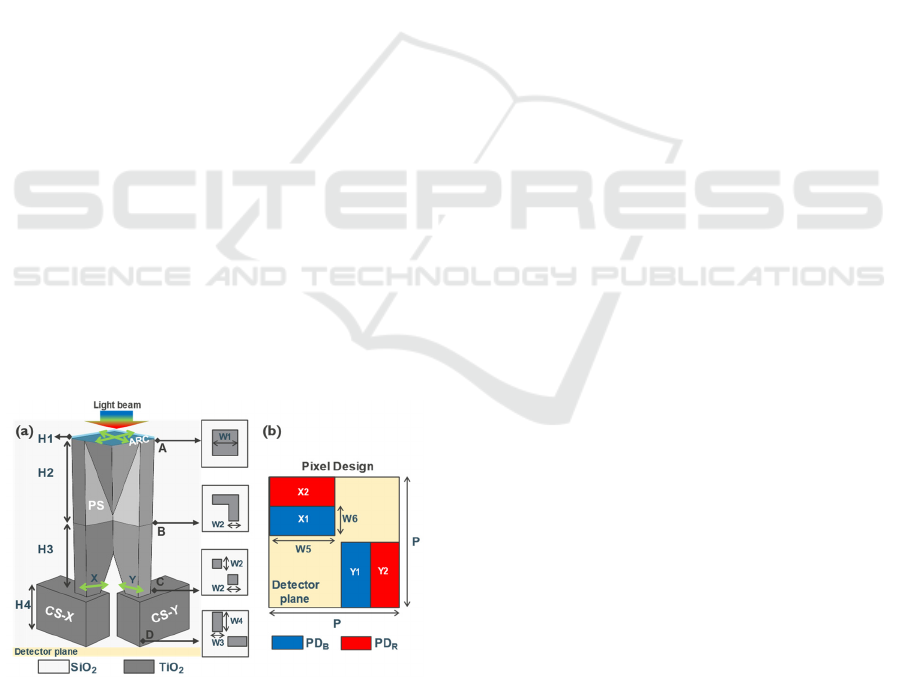
Figure 1 shows a schematic representation of the
proposed polarization color router (PCR). A sketch of
the unit cell design with a pitch P is depicted in Figure
1a. The PCR is composed of two optical components
with distinct functionalities: a polarization splitter
(PS) unit on top and color splitter (CS-X, CS-Y) unit
below. Both units are composed of high index
vertical-waveguides with TiO
2
as a core and a SiO
2
cladding. The corresponding geometric parameters
and cross-sectional views are presented at multiple
planes (A–D) along the propagation direction.
The primary function of the top PS is to route the
input light beam to distinct output channels according
to its polarization state. It comprises of two segments:
a top square-shaped input waveguide (plane A) with
thickness H2 and width W1, which tapers down
asymmetrically to two partially overlapping
orthogonal waveguides of dimension W1×W2
forming an L-shaped cross section at plane B. The
bottom segment consists of an L-shaped waveguide
of thickness H3, which gradually tapers down to two
orthogonal square-shaped waveguides of width W2
(at plane C). The input waveguide adiabatically
transmits the light beam to the L-shaped waveguide
at plane B. Then, the beam is routed towards either of
the square-shaped waveguides X or Y at exit plane of
the PS (plane C), based on the incident polarization
vector's orientation (horizontal or vertical
polarization: indicated by green arrows).
Figure 1: Schematic of the Polarization Color Router: (a) A
unit cell design comprising vertical-waveguides with cross-
sectional views at different planes. (b) A configuration for
the pixel design at the detector plane for a unit cell with a
pitch P = 1 µm.
Bottom color splitting elements (CS-X, CS-Y)
separate the incident light signal into its constituent
wavelengths or colors at sub-micron spatial
resolution. To achieve this functionality multimode
vertical-waveguides are employed, a technology
previously validated in our earlier research (Kang et
al., 2023). The color splitting segment consists of two
identical rectangular waveguides with dimension W3
× W4 × H4, connected to the two orthogonal output
channels of the top PS unit at plane C. The PS exit
waveguide (X or Y) injects light asymmetrically into
the color splitting element (CS-X or CS-Y), exciting
both fundamental and second-order modes within the
waveguide. As these modes propagate, their speeds
vary with frequency causing spatial separation of
colors at the waveguide exit (plane D). It is worth to
mention, a subtle tuning of the waveguide’s
geometric parameters enables a precise control over
the optimal color spectrum, demonstrating the
versatility of our device. Finally, the separated colors
(polarization dependent) are captured by
corresponding pixels in the detector plane.
The device also features an H1 thick anti-
reflection coating (ARC) layer on waveguide
entrances to effectively reduce the back reflections
and enhance device efficiency. When illuminated
with a focused light beam from the top, device splits
the beam into constituent color bands according to its
polarization state, subsequently recorded in the
relevant pixel. Here, the visible spectrum is divided
into two bands (Blue/Red), with the potential to
expand to three bands (RGB) by adjusting the
waveguide’s dimension. The proposed pixel design is
composed of four pixels in a compact layout at the
detector plane, labelled X1, X2, Y1, and Y2, with
dimensions W5ൈ W6, as shown in Figure 1b. The
pixel pairs (X1, X2) and (Y1, Y2) are designed to
capture blue and red spectral bands for X-polarized
and Y-polarized light, respectively.
Finite difference time domain simulations in a
commercial solver, were employed to perform a
comprehensive optimization of design parameters
and analyse the optical performance of PCR (Ansys
Lumerical FDTD). A broadband Gaussian beam of
numerical aperture (NA) 0.8 was used to excite the
proposed device across the visible spectrum 400-700
nm. Unit cell simulations were performed with Bloch
boundary conditions in X and Y directions, while
perfectly matched layer (PML) boundary conditions
were set for the Z axis (propagation direction). The
optical constants of SiO
2
and TiO
2
used for
simulations
were taken from in-house measurements
and presented in the Figure 2.
PHOTOPTICS 2025 - 13th International Conference on Photonics, Optics and Laser Technology
16
The optimal device parameters were determined
through a two-stage nested sweeps simulation
process, targeting maximum efficiency and low pixel
cross-talk as main figure of merit. Initially, the top PS
unit was optimized for maximum polarization routing
efficiency, yielding optimal design parameters: P =1
μm, W1 = 550 nm, W2 = 200 nm, H2 = 2.8 μm, and
H3 = 3.7 μm. Subsequently, optimization of color
splitting elements enabled the separation of the
polarization-routed beam into two spectral bands,
leading to corresponding parameters: W3 = 200 nm,
W4 = 400 nm, and H4 = 3.1 μm. ARC design
principle and numerical optimization led to the
selection of a 90 nm thick (H1) SiO
2
layer as the
optimal anti-reflective coating. Meanwhile,
subwavelength pixel dimensions of W5 = 225 nm and
W6 = 500 nm were employed, yielding high spatial
resolution.
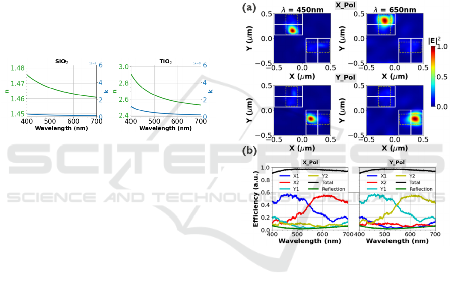
Figure 2: Material Optical Constants: Refractive Index (n,
k) of SiO
2
and TiO
2
.
3 RESULTS AND DISCUSSION
Figure 3 shows the simulated optical performance of
the proposed device under broadband visible
illumination (400-700 nm). The simulated electric-
field intensity distribution at the detector plane is
presented in Figure 3a, showing the device’s response
to blue (450 nm) and red (650 nm) wavelengths for
both X and Y polarization states. For X-polarization,
the incident light is primarily directed to the X output
channel at the PS exit (plane C: Figure 1a), then
routed to the CS-X splitting element where blue and
red wavelengths propagate at different speeds and are
separated into X1 and X2 pixels as evident from the
top row of Figure 3a. In contrast, Y1 and Y2 capture
the aforementioned colors for the orthogonal (Y)
polarization state (bottom row). Meanwhile, it is
worth to mention that for all four possible
configurations, the field is highly localized in the
designated pixels ensuring high efficiency with
minimal polarization and color crosstalk.
Figure 3b shows the spectral response of the PCR
for orthogonal polarization states of the incident light
beam. It can be observed that for X-polarization, the
majority (≈50%) of light in the blue band (400-550
nm) is collected by the X1 pixel, meanwhile X2
captures the red band (550-700 nm) with a similar
efficiency. The geometric symmetry induces a similar
response for the orthogonal polarization state (on the
right side of Figure 3b but now with Y1 and Y2 active
pixels. Average cross-talk between the active pixels
across the two spectral bands is 35-40%, which can
be further supressed by introducing deep trench
isolation (DTI) between the pixels. The device
achieves remarkable efficiency, featuring high
(>95%) total transmission and low (<5%) reflection.
Moreover, the device exhibits a low power leakage,
with under 5% of power directed to pixel-free region.
Figure 3: Optical performance of the PCR: (a) Normalized
electric-field intensity distribution profiles at the detector
plane for orthogonal polarization states (X and Y) at 450 nm
and 650 nm. The white (solid) and yellow (dashed)
rectangles define the four pixel and bottom color splitters
perimeters. (b) Transmission and reflection efficiency for X
and Y-polarized incident light over the visible spectrum.
Next, we demonstrate the device's versatility by
tuning the short-axis width (W3) of color splitting
units (CS-X, CS-Y) to support multiple color
compositions. For this purpose, simulations were
performed by sweeping W3 from 150 nm to 250 nm,
using an X-polarized Gaussian beam (NA = 0.8).
Figure 4 illustrates the dependance of pixel (X1, X2)
transmission efficiency over incident beam’s
wavelength and waveguide’s short-axis width. These
transmission maps indicate a gradual shift of the
crossing point (identified by black arrows) of two
separated spectral bands, defining the color
Design and Simulation of a Vertical Waveguide Based Polarization Color Routing Device
17
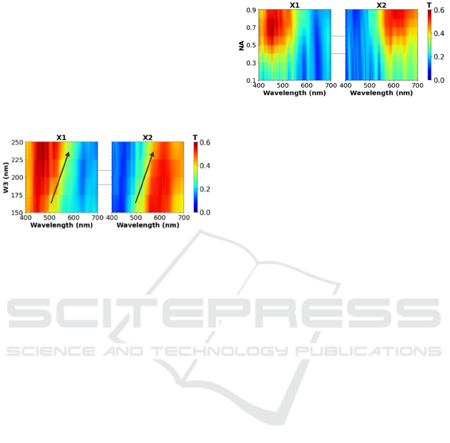
information in the relevant pixel. With a short-axis
width of 150 nm, wavelengths between 400-500 nm
were directed to pixel X1 and X2 received 500-700
nm, whereas the 250nm width split the spectrum into
400-570 nm (X1) and 570-700 nm (X2), without any
significant loss in the routing efficiency. Thus, by
precise control over short-axis width, the desired
color composition can be achieved. Furthermore,
tailoring thickness (H4) and long-axis width (W4) can
offer additional degree of freedom to achieve
customized spectral splitting.
Figure 4: Variation of pixel’s spectral composition: Power
transmission to the X1 and X2 pixel as a function of
wavelength and short axis width of bottom color splitting
unit.
To analyze the device’s capability to operate
under different illumination conditions, it was excited
with an X-polarized Gaussian beam by varying the
numerical aperture between 0.1-0.9. Figure 5 depicts
the power routed to the corresponding pixels (X1, X2)
as a function of wavelength and numerical aperture.
It is evident that the device performs as intended and
separates the two wavelength bands (blue and red) for
all illumination numerical apertures, albeit with
changes in efficiency. Although, pixel’s transmission
efficiency drops as NA decrease, yet remains ≈25%
for the lowest designed NA of 0.1. Nonetheless, we
anticipate that by following the optimization process,
the device can be tailored to operate at desired NA
with high routing efficiencies.
Further investigation will focus on expanding the
device's capabilities to separate polarization-
dependent visible light into red, green, and blue
(RGB) spectral bands by tailoring the color splitting
waveguide's geometric dimensions. While the bottom
color splitters have already been successfully
fabricated using standard backend processing
techniques on 300 mm wafers (Kang et al., 2023), we
will explore advanced lithography and fabrication
techniques to develop top polarization splitting
waveguides to realize complete device stack.
Ultimately, optical characterization will be performed
to determine the device's true efficiency and validate
its performance.
Figure 5: Device performance under a wide range of
illumination numerical aperture (NA) settings: Power
transmitted to the X1 and X2 pixel as a function of designed
numerical aperture and wavelength.
4 CONCLUSION
In conclusion, a novel high index vertical-waveguide
based polarization color routing device at visible
wavelengths is proposed and investigated through
numerical simulations. The key innovation lies in
simultaneously splitting the polarization and color at
sub-micron spatial resolution with near unity
transmission and a high pixel routing efficiency of
50%. The design’s versatility enables a tuneable color
composition via geometric parameter modulation and
adoptability to perform well over a wide range of
numerical aperture settings. We firmly believe this
device shows great promise to be implemented for
high NA polarization-sensitive image sensors with
possible applications in high-end professional
cameras, smartphones, and machine vision devices.
REFERENCES
Park, S., Lee, C., Park, S., Park, H., Lee, T., Park, D., Heo,
M., Park, I., . . . & Kim, T. (2022). A 64Mpixel CMOS
Image Sensor with 0.56μm Unit Pixel Separated by
Front Deep-Trench Isolation. IEEE International Solid-
State Circuits Conference (ISSCC), San Francisco, CA,
USA, pp. 1-3. https://doi.org/10.1109/ISSCC42614.
2022.9731750.
Theuwissen A. (2021). There’s More to the Picture Than
Meets the Eye, and in the future it will only become
more so. IEEE International Solid-State Circuits
Conference (ISSCC), San Francisco, CA, USA, pp. 30-
35. https://doi.org/10.1109/ISSCC42613.2021.936605.
Takahashi, S., Huang, Y-M., Sze, J-J., Wu, T-T., Guo, F-
S., Hsu, W-C., . . . & Yaung, D-N. (2017). A 45 nm
Stacked CMOS Image Sensor Process Technology for
Submicron Pixel. Sensors, 17(12), 2816. https://doi.org
/10.3390/s17122816.
Gruev, V., Perkins, R., & York, T. (2010). CCD
polarization imaging sensor with aluminum nanowire
PHOTOPTICS 2025 - 13th International Conference on Photonics, Optics and Laser Technology
18

optical filters. Opt. Express 18, 19087-19094. https://
doi .org/10.1364/OE.18.019087.
Chen, W. T., Török, P., Foreman, M. R., Liao, C. Y., Tsai,
W-Y., Wu, P. R., & Tsai, D. P. (2016). Integrated
plasmonic metasurfaces for spectropolarimetry.
Nanotechnology 27 224002. https://doi.org/10.1088/
0957-4484 /27/22/224002.
Wu, Y., Yang, Y., Yin, Y., Dai, L., Li, X., Huang, H., &
Wen, S. (2023). Flexible high-resolution thin
micropolarizers for imaging polarimetry. Chin. Opt.
Lett. 21, 031301. https://doi.org/10.3788/COL202321
.031301.
Arbabi, E., Kamali, S. M., Arbabi, A., & Faraon, A. (2018).
Full-Stokes Imaging Polarimetry Using Dielectric
Metasurfaces. ACS Photonics, 5 (8), 3132–3140.
https://doi. org /10.1021/acsphotonics.8b00362.
Lee, G-D. R., Kim, D-H., Kwon, D., Park, J-E., Cho, D.,
Kang, J., . . . & Song, J. (2023). A 0.5µm Pixel 3-layer
Stacked CMOS Image Sensor with Deep Contact and
In-pixel Cu-Cu Bonding Technology. International
Electron Devices Meeting (IEDM), San Francisco, CA,
USA, pp. 1-4. https://doi.org/10.1109/IEDM45741.
2023.10413687.
Scott-Thomas, J. (2023). Trends and Developments in
State-of-the-Art CMOS Image Sensors. https://www.
imagesensors.org/Past%20Workshops/2023%20Work
shop/2023%20Papers/R1.pdf
Nishiwaki, S., Nakamura, T., Hiramoto, M., Fujii, T., &
Suzuki, M. (2013). Efficient colour splitters for high-
pixel-density image sensors. Nature Photon, vol. 7, no.
3, pp. 240–246. https://doi.org/10.1038/nphoton.
2012.345.
Yun, S., Roh, S., Lee, S., Park, H., Lim, M., Ahn, S., &
Choo, H. (2021). Highly Efficient Color Separation and
Focusing in the Sub-micron CMOS Image Sensor.
IEEE International Electron Devices Meeting (IEDM),
San Francisco, CA, USA, pp. 30.1.1-30.1.4. https://doi.
org/10.1109/IEDM19574.2021.9720592.
Kang, S., Benelajla, M., Ciamain, R. M., Ali, F.,
Papadopoulou, A., . . . & Genoe, J. (2023). Wafer-level-
integrated vertical-waveguide sub-diffraction-limited
color splitters. International Electron Devices Meeting
(IEDM), San Francisco, CA, USA, pp. 1-4. https://doi.
org/10.1109/IEDM45741.2023.10413746.
Khorasaninejad, M., Zhu, W., & Crozier, K. B. (2015).
Efficient polarization beam splitter pixels based on a
dielectric metasurface. Optica 2, 376-382. https://doi.
org /10.1364/OPTICA.2.000376.
Rubin, N. A., D’Aversa, G., Chevalier, P., Shi, Z., Chen,
W. T., & Capasso, F. (2019). Matrix Fourier optics
enables a compact full-Stokes polarization camera.
Science365, eaax1839. https://doi.org/10.1126/science
.aax1839.
Nesic, A., Blaicher, M., Marin-Palomo, P., Füllner, C.,
Randel, S., Freude. W., & Koos, C. (2023). Ultra-
broadband polarisation beam splitters and rotators
based on 3D-printed waveguides. Light: Advanced
Manufacturing 4, 23. https://doi.org/10.37188/lam.
2023.022.
Ansys Lumerical FDTD. https://www.ansys.com/products
/optics/fdtd.
Design and Simulation of a Vertical Waveguide Based Polarization Color Routing Device
19
