
A Low-Noise Amplifier in Submicron CMOS for
Neural Recording on Optogenetics Applications
H. E. Oshiro
1,2 a
, R. A. P. Andrade
2 b
, J. N. S. Junior
1 c
, M. Luppe
1 d
,
E. Colombari
3 e
, M. C. Dias
4 f
and J. P. Carmo
1 g
1
Group of Metamaterials Microwaves and Optics (GMeta), Department of Electrical Engineering (SEL), University of São
Paulo (USP), Avenida Trabalhador São-Carlense, Nr. 400, São Carlos 13566-590, SP, Brazil
2
brain4care, Avenida Bruno Ruggiero Filho, 971 - Parque Santa Felícia Jardim, São Carlos, SP, 13562-420, Brazil
3
Department of Physiology and Pathology, Faculty of Odonthology, São Paulo State University (UNESP), Rua Humaitá,
Nr. 1680, Araraquara 14801-385, SP, Brazil
4
Faculty of Medicine, University of Porto, Alameda Hernani Monteiro, piso 8, Unidade Cuidados Neurocriticos,
{helder.oshiro, na rade@gmail.com,
eduardo.colombari@unesp.br, mcdias@med.up.pt
Keywords: Low-Noise Amplifier, Bioamplifier, CMOS, Optogenetics, Neuronal Signal.
Abstract: Optogenetics combines optical and genetic techniques to control and monitor neuronal activities. Recent
efforts seek the development of portable and even wireless electronics for optical activation and acquisition
of biopotentials, aiming to offer greater mobility and freedom to study animals, in contrast to the large
equipment commonly found in laboratories that perform the activation of lasers, signal amplifiers and
acquisition. In this context, this paper reports on the design and simulation of a low-noise amplifier (LNA) to
acquire neural signals on optogenetics applications. The simulations showed that with the nominal voltage
supply of 1.8V this LNA is able to amplify neuronal signals in the range of 0.3Hz up to 172kHz with a gain
of 39.3dB, while rejecting DC offsets generated at the interface between the electrodes. The simulations also
showed that with variations of 20% with relation to the nominal voltage supply, the worse cases of the lower
and higher cut-off frequencies were 0.3Hz (increased) and 51.3kHz (decreased), respectively. Moreover,
under these stressing conditions the gain had a variation between 36.8dB for the worst scenario and 40dB
for the best scenario. These results are more than enough to meet the bandwidth requirements on optogenetics
and it can be concluded that the specifications of the LNA are not affected by the useful life of batteries under
the aforementioned voltage variation range. The power consumption of the system is around 64μW from a
1.8V voltage supply. This LNA was designed in the 6-metals/1-poly 0.18m CMOS process from UMC
(United Microelectronics Corporation) and occupies an area of 0.092mm
2
.
1 INTRODUCTION
The Optogenetics combines optical and genetic
techniques to control and monitor neuronal activities
(Deisseroth, 2011). Recent efforts seek the
development of portable and even wireless
electronics for optical activation and acquisition of
a
https://orcid.org/0000-0003-0370-4700
b
https://orcid.org/0000-0002-7248-4636
c
https://orcid.org/0000-0002-1975-2267
d
https://orcid.org/0000-0001-7419-2154
e
https://orcid.org/0000-0002-1395-4036
f
https://orcid.org/0000-0003-0340-9808
g
https://orcid.org/0000-0001-7955-7503
biopotentials, aiming to offer greater mobility and
freedom to study animals, in contrast to the large
equipment commonly found in laboratories that
perform the activation of lasers, signal amplifiers and
acquisition. For this reason, the optogenetics is an
emergent field of applications, where the signals are
acquired from a specific part of the brain and at the
1080
Oshiro, H. E., Andrade, R. A. P., S. Junior, J. N., Luppe, M., Colombari, E., Dias, M. C. and Carmo, J. P.
A Low-Noise Amplifier in Submicron CMOS for Neural Recording on Optogenetics Applications.
DOI: 10.5220/0013147200003911
Paper published under CC license (CC BY-NC-ND 4.0)
In Proceedings of the 18th International Joint Conference on Biomedical Engineering Systems and Technologies (BIOSTEC 2025) - Volume 1, pages 1080-1084
ISBN: 978-989-758-731-3; ISSN: 2184-4305
Proceedings Copyright © 2025 by SCITEPRESS – Science and Technology Publications, Lda.
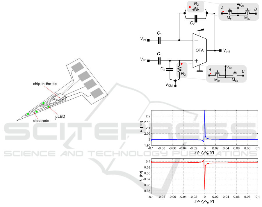
same time this same part can also be stimulated with
light and, in this context, Figure 1(a) shows the
concept of electrode with a chip-in-the-tip for
optogenetics, where a bio-amplifier and the
respective signal processing/control/interface
electronics simultaneously acquires the neuronal
signals and stimulates through light. This paper
presents the design of a fully integrated bio-amplifier
suitable for recording biological signal within the
range of 1Hz up to 10kHz that was designed in the
6-metals/1-poly 0.18m CMOS process from the
UMC. The simulations showed that these
specifications were met for the nominal voltage of
1.8V, even with the LNA stressed with high
variations of 20%.
Figure 1: Illustration of the chip-in-the-tip concept for
application in optogenetics.
2 CIRCUIT DESIGN
2.1 Pseudoresistors and Amplifier
Elements
Figure 2 shows the schematic of the proposed LNA,
which is composed by an Operational
Transconductance Amplifier (OTA) and few discrete
passive components. The resistors R
2
are in fact MOS-
bipolar devices, where each one is composed by two
PMOS transistors connected in series with their bulks
and gates connected to the supply rail V
dd
and their
sources tied together. These two pairs of two PMOS
form two pseudo-resistors, whose implementation is
also depicted in Figure 2 (Harrison et al., 2003)
(Wattanapanitch et al., 2007). The pseudoresistors are
in the order of T, and they are called ‘pseudo’
because it mimcs the behavior of a real resistor. The
parallel of R
2
with C
2
creates a pole in the transfer
function (the gain is frequency dependent) with the
frequency f
L
=(2R
2
C
2
)
-1
with low-pass behaviour.
Therefore, R
2
must be in the order of T to compensate
for the fact that C
2
is in the order of fF to ensure that f
L
is located as close as possible to the origin and the most
as possible smaller than 1Hz that contains neuronal
information. This amplifier is also composed by two
capacitors (C
1
25.8pF and C
2
206fF) and by a
transconductance operational amplifier (OTA). In the
end, the voltage gain of this amplifier is
A
V
=C
1
/C
2
=100=40dB.
Figure 2: Schematic of the LNA, highlighting the pseudo-
resistors components.
Figure 3: Resistance response of the pseudo-resistors (top
plot) and the pole location f
L
[Hz] in the transfer function of
the LNA (bottom plot) versus the voltage input.
The top plot of Figure 3 shows the simulated
resistance response of the pseudo-resistors in terms of
the voltage ΔV=V
in
-V
out
at its terminals, where V
in
is
the terminal that connects to the bulk of the first
PMOS and Vout is the terminal that connects to the
gate of last PMOS (in concordance with Figure 2). A
voltage pulse source was placed between the V
in
and
V
out
terminals of the pseudo-resistor, and the voltage
were varied between -0.1 V and +0.1 V. The current
was simulated obtained, and the resistance was
calculated by dividing the voltage by the current. The
bottom plot of Figure 3 shows the pole location
A Low-Noise Amplifier in Submicron CMOS for Neural Recording on Optogenetics Applications
1081
f
L
[Hz] in the transfer function of the LNA (bottom
plot) versus the voltage input. One conclusion comes
to light, the lower cut-off frequency f
L
more than
meets the lower bond specification of the LNA, e.g.,
f
L
«1Hz for any voltage in the range [-0.1,0.1] V.
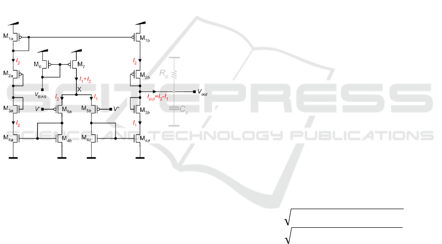
2.2 Design of the Operational
Transconductance Amplifier
(OTA)
Figure 4 illustrates the schematic of the OTA, which
is composed by eight p-type and six n-type
transistors. The output into/from the load capacitor C
is given by I
out
=g
m
.(V
+
-V
-
), where g
m
[S] is the
transconductance of the OTA, V
+
corresponds to the
positive input (V
IP
) and V
-
to the negative input
(V
IM
) in Figure 2. The circuit of the OTA operates
from a 1.8V power supply, and the common mode
voltage is set to V
CM
=V
dd
/2=0.9V.
Figure 4: Schematic of the OTA and currents (I
1
=I
2
) for all
MOSFETs saturated in strong inversion.
Since V
+
=V
CM
+in
+
and V
-
=V
CM
+in
-
and |in
,+
|«V
CM
(frequently, in
-
=-in
+
), thus V
X
constant. For in
+
>in
-
:
I
2
>I
1
. The DC voltage of V
sg
is the same for M
1b
and
M
1a
, thus I
2
>I
1
, forcing:
I
out
=I
2
-I
1
>0
(1)
and
V
out
=(I
out
/C).t>0
(2)
In the opposite situation, for in
+
<in
-
, the currents
are such that:
I
out
=I
2
-I
1
<0
(3)
and
V
out
=(I
out
/C).t<0
(4)
To obtain the output voltage V
out
in terms of the
diferential input V
in
=(V
+
-V
-
)=(in
+
-in
-
), I
1
and I
2
must
be obtained. The currents are then:
I
1
=1/2.
p
C
ox
(W/L).(V
+
-V
X
+V
thp
)
2
(5)
with (W/L)=(W/L)
5
and
I
2
=1/2.
p
C
ox
(W/L).(V
X
-V
-
+V
thp
)
2
(6)
In this case. the output voltage isgiven by:
V
out
(t)=V
0
+(I
2
-I
1
)/C.t
(7)
where V
0
is the abstract inicial condition/voltage. The
signals to amplify are such that |in
-,+
|«V
CM
, meaning
that:
V
out
(t)V
0
+[2
p
C
ox
(W/L).(V
X
-V
CM
+V
thp
)
(in
-
-in
+
)/C]t=
=V
0
-[2
p
C
ox
(W/L).(V
X
-V
CM
+V
thp
)/C]
V
in
t
(8)
The voltage variation V
out
=V
out
(t)-V
0
in terms of the
voltage V
in
=in
+
-in
-
is given by:
V
out
=2
p
C
ox
(W/L)(V
X
-V
CM
+V
thp
)(t/C)
(in
+
-in
-
)=
=K.(in
+
-in
-
)
(9)
The equation (9) is true for
=0 (without the
channel length modulation effect). Nonetheless, even
with
0, the equation (9) is still true if R
o
is high (in
the order of M). This resistance can be tuned
according the following equation:
R
o
=R
o1
//R
o2
=
={r
o3b
+r
o4d
.[1+g
m3b
.(1+
).r
o3b
]}//
//{r
o2b
+r
o1b
.[1+g
m1b
.(1+
).r
o2b
]} [M]
(10)
with
==
==
−
−
1
DC,2,121
1
DC,2,143
)(
)(
Irr
Irr
pbobo
ndobo
(11)
and
=
=
DC,2,133
DC,2,122
)/(2
)/(2
ILWCg
ILWCg
boxnbm
boxpbm
(12)
The transconductance of this OTA is given by:
g
m
=2
p
C
ox
(W/L)(V
X
-V
CM
+V
thp
)=g
m5
(13)
with
g
m5
=[2
p
C
ox
(W/L).I
1,2,DC
]
½
(14)
2.3 LNA Behaviour: Transfer Function
H
LNA
(F)=V
out
/(V
IP
-V
IM
)
The LNA faces several challenges due to the nature
of the signals to amplify that are characterized by
low-amplitudes and low-frequencies very close to the
DC component. These types of amplifiers typically
EM4Health 2025 - Special Session on Electromagnetic waves for healthcare
1082
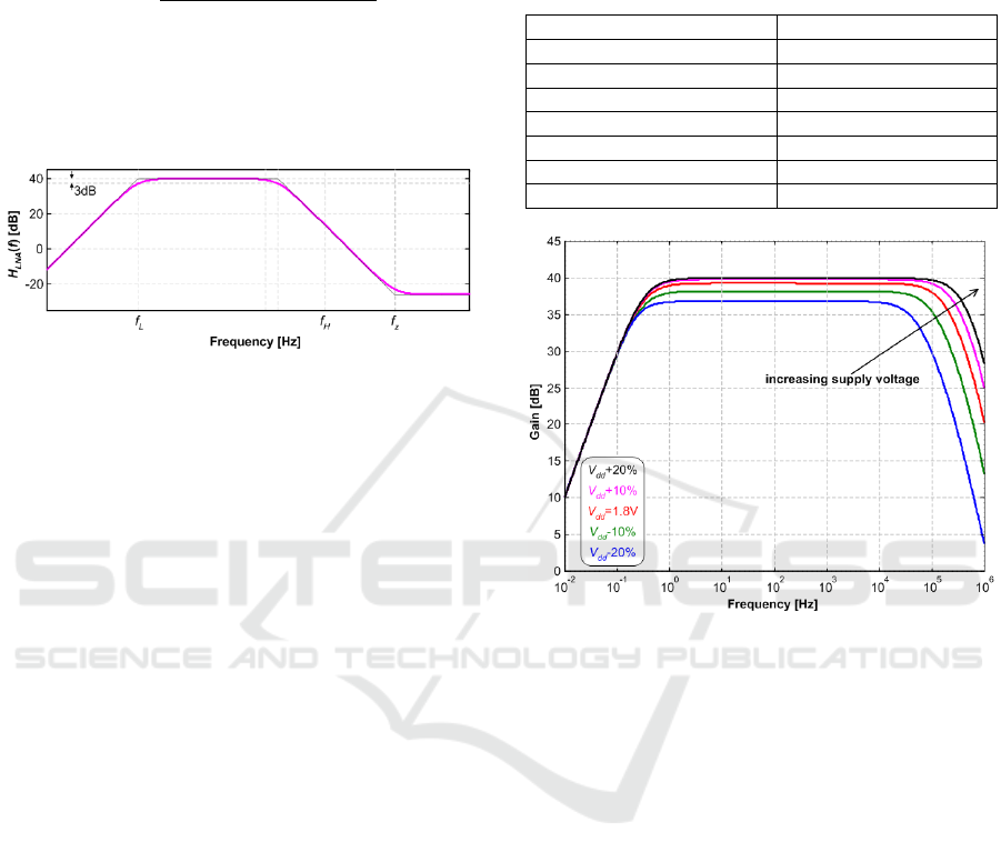
present a mid-band gain of about 40dB, and as stated
before, a bandwidth ranging from the 1Hz to 10kHz.
The transfer function H
LNA
(f) of the LNA is given by:
)2).(2(
)2.(
)(
Hz
z
LNA
fsfs
fss
sH
++
−
−=
(15)
Figure 5 depicts the theoretical Bode diagram of
H
LNA
(f) of the LNA, whose transfer function contains
two zeros and two zeros.
Figure 5: Theoretical Bode diagram of the transfer function
H
LNA
(f) of this LNA.
One zero is located in the origin, while the other
is located at f
z
=g
m
/(2πC
2
). As stated before, the
smallest pole is located in the lower cut-off frequency
f
L
=1/(2πR
2
C
2
), while the highest pole is located in the
upper cut-off frequency f
H
=g
m
/(2πC
1
). It must be
noted that the frequency of the second zero f
z
is much
higher than the frequency of any pole. As expected,
the LNA gain between f
L
and f
H
can be determined
and as already known, it is approximately given by
(C
1
/C
2
). Table 1 lists the dimensions of the
MOSFETs that comprises the OTA and the pseudo
resistors.
Capacitors C
1
and C
2
were implemented with
MIMcaps, which use the Metal 6 and Metal 5 layers
as the capacitor’s plates. The overlap capacitance
already include the fringe field and measures
1fF.m
-1
(Europractice, 2025). The option of the
used technology was the mini@SIC prototipation.
This option offers a shalow trench isolation (STI),
triple well, aluminium interconnects for all metals,
metal 6 as top metal with a thickness of 20kÅ
(e.g., 2m) (Europractice, 2025).
3 RESULTS
The simulations done with the nominal voltage
supply of 1.8V showed a midband gain of 39.3dB in
the range from 0.3Hz to 172kHz. Figure 6 shows the
frequency response. Below 0.3Hz the loss of gain is
approximately 3dB.
Table 1: Dimensions of the MOSFETs that comprises the
OTA and the pseudo resistors.
MOSFET
Total (W/L)
M
1a
, M
1b
13.4 μm/20 μm
M
2a
, M
2b
20.6 μm/0.28 μm
M
3a
, M
3b
15.4 μm/0.28 μm
M
4a
, M
4b
, M
4c
, M
4d
10 μm/20 μm
M
5a
, M
5b
463 μm/0.51 μm
M
6
, M
7
2.3 μm/5.1 μm
Pseudo-resistors M
p1
to M
p6
1 μm/1 μm
Figure 6: Simulation results with the gain of LNA and
respective transfer function H
LNA
(f).
Few stress tests were applied to the LNA, varying the
supply voltage by 10% and 20% in relation to the
nominal value. The simulations also showed that the
variation in the lower cut-off frequency f
L
was not
significant but was advantageous, because it reduced
from 0.3Hz to 0.2Hz when the supply voltage
dropped by 20% in relation to the nominal value. On
the other hand, the 20% decrease in supply voltage
resulted in the largest reduction in the upper cutoff
frequency f
H
from 172kHz to 51kHz. In the opposite
situation, when the supply voltage increases by 20%,
this frequency f
H
increases from 172kHz to 355kHz.
The gain of LNA varied from 39.3dB to 40dB and
36.8dB, when the supply voltage varied from +20%
and -20%, respectively. In resume, the bounds f
L
and
f
H
, as well as, the bandwidth BW=f
L
-f
H
of the gain are
more than enough to cover the range of extracellular
recorded spikes from 1Hz to 10kHz. Figure 6 also
shows the gains for each stress test.
A Low-Noise Amplifier in Submicron CMOS for Neural Recording on Optogenetics Applications
1083
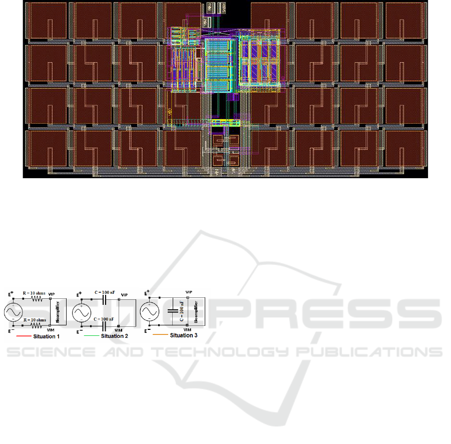
Figure 8: Layout of this LNA.
As illustrated in Figure 7, three different scenarios
were also simulated to analyse the robustness of the
LNA considering the capacitance and resistance
associate to the wires that connect the electrodes to
the input of LNA.
Figure 7: Scenarios for the robustness simulation of LNA.
The resistance was considered around 10Ω in
Situation 1. This value is probably higher than the
real, but it was an extrapolated value to confirm the
previous robustness of the amplifier.The capacitance
was considered around 100nF in both Situations 2 and
3. Situation 1 considered a serial resistance existent
between the positive electrode E
+
and the positive
input of the LNA (V
IP
), and the one between E
-
and
V
IM
. Situation 2 considered a capacitor in series with
both positive and negative electrodes. Finally,
Situation 3 considered a capacitor placed in parallel
to the voltage source.
The three scenarios were simulated for the several
voltage supplies described latter. The simulation
results revealed that, for a given voltage supply, the
gain and the frequencies f
L
and f
H
were not affectd for
these parasitics that may are present in the connection
wires between the electrodes and the LNA. These
results are important because allows to get the
conclusion that this LNA is very reliable and robust
to external electrical factors on wires.
4 CONCLUSIONS
This paper presented a low-noise amplifier (LNA)
that was optimized for use on acquisition of neural
signals on optogenetics applications. This LNA is
part of a more complete microdevice, comprising
optical neurostimulation to meet the need of more
compact solutions for research laboratories. Figure 8
shows the layout of the proposed LNA, which
occupies an area of silicon of 200m460m.
ACKNOWLEDGEMENTS
This work was partially supported by the CNPq
through the project with the reference
CNPq 402752/2023-6 and the PQ scholarship with
the reference CNPq 305858/2023-8.
REFERENCES
Deisseroth, K. (2011). Optogenetics, Nature Methods,
Vol. 8, No. 1, pp. 26-29.
Harrison, R.R.; Charles, C. (2003). A low-power low-noise
cmos for amplifier neural recording applications. IEEE J.
Solid-State Circuits, 38, 958–965.
Wattanapanitch, W.; Fee, M.; Sarpeshkar, R. (2007). An
Energy-Efficient Micropower Neural Recording
Amplifier. IEEE Trans. Biomed. Circuits Syst., 1, 136–
147.
Europractice (2025). Europractice IC Service, UMC
Technologies, [on-line] https://europractice-ic.com/,
accessed on 17
th
January 2025.
EM4Health 2025 - Special Session on Electromagnetic waves for healthcare
1084
