
Advancing Detector Shielding with Thermo-Optic Defocusing in
PMMA Integrated on Silicon Nitride
Soon Thor Lim
1 a
, Thomas Ang
1 b
, Zifeng Yuan
2
, Thanh Xuan Hoang
1 c
, Dewen Zhang
2 d
,
Ching Eng Png
1 e
, Aaron Danner
2 f
and Gandhi Alagappan
1 g
1
Institute of High Performance Computing, Agency for Science, Technology and Research, Singapore
2
Dept. of Electrical and Computer Engineering National University of Singapore, Singapore
Keywords: Thermo-Optic Defocusing, Polymethyl-Methacrylate (PMMA), Optical Power Limiter (OPL).
Abstract: This study develops an on-chip optical power limiter (OPL) based on the thermo-optic defocusing effect in
PolyMethyl-Methacrylate (PMMA) to protect an avalanche photodiode (APD) from high optical power
damage. The OPL is designed to operate within a reduced power range of 0.1 mW to 10 mW by adjusting
waveguide dimensions, taper widths, and free-space region (FSR) lengths. Detailed calculations, modelling,
and simulations are presented, demonstrating the efficacy of the OPL in limiting optical power reaching the
APD, preventing damage and ensuring stable performance in high-power applications.
1 INTRODUCTION
Silicon photonics plays a pivotal role in data
communications, quantum key distribution (QKD),
and sensing applications. As these systems evolve,
protecting photonic circuits from high-intensity
optical signals becomes crucial, particularly for
safeguarding sensitive components like avalanche
photodiodes (APDs). Optical Power Limiters (OPLs)
(Lee, 1993) are essential for preventing damage from
excessive power and ensuring stable operation. While
technologies such as silicon waveguides with strong
two-photon absorption (Osgood, 2009) and photonic
crystals (Zheng, 2015) face limitations in integration
and fabrication, polymer-based OPLs, like those
using PMMA (Gandhi, 2024), offer advantages in
thermal management and power handling. This paper
presents a PMMA-based OPL design using the
thermo-optic defocusing effect to protect APDs,
ensuring reliable performance and extending device
a
https://orcid.org/0000-0003-2350-823X
b
https://orcid.org/0000-0002-1914-988X
c
https://orcid.org/0000-0002-6815-487X
d
https://orcid.org/0009-0005-5426-5869
e
https://orcid.org/0000-0002-7797-1863
f
https://orcid.org/0000-0002-9090-9626
g
https://orcid.org/0000-0002-4730-2503
lifespan in variable environments. Avalanche
photodiodes (APDs) are widely used in high-speed
optical communication systems due to their high
sensitivity. However, they are prone to damage when
exposed to optical powers beyond a few milliwatts.
Therefore, an optical power limiter (OPL) is essential
to protect APDs from high intensity light. In this
paper, we design an OPL that operates in the power
range of 0.1 mW to 10 mW. The OPL employs a
thermo-optic defocusing mechanism in PMMA, a
material with a negative thermo-optic coefficient.
This mechanism induces beam divergence with
increasing input power, which limits the amount of
light reaching the APD. Building on the principles
from our high-power OPL designs, we reduce the
maximum limiting power range from 10 mW - 102
mW to 0.1 mW - 10 mW.
92
Lim, S. T., Ang, T., Yuan, Z., Hoang, T. X., Zhang, D., Png, C. E., Danner, A. and Alagappan, G.
Advancing Detector Shielding with Thermo-Optic Defocusing in PMMA Integrated on Silicon Nitride.
DOI: 10.5220/0013148400003902
In Proceedings of the 13th International Conference on Photonics, Optics and Laser Technology (PHOTOPTICS 2025), pages 92-94
ISBN: 978-989-758-736-8; ISSN: 2184-4364
Copyright © 2025 by Paper published under CC license (CC BY-NC-ND 4.0)
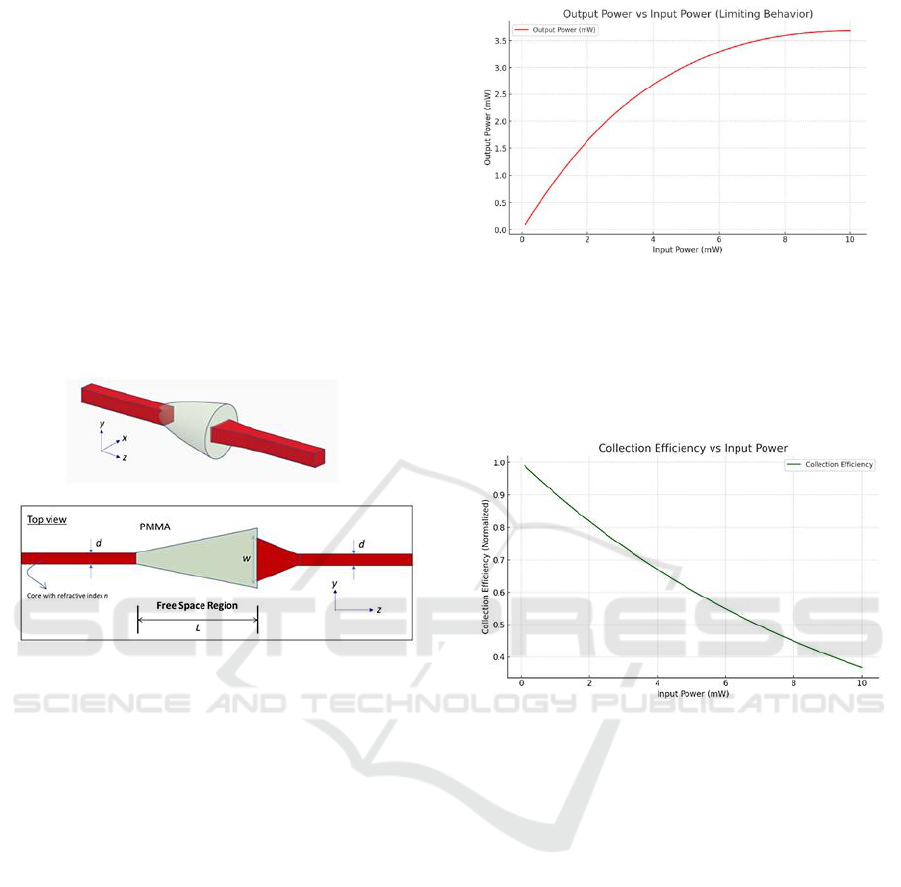
2 OPL DESIGN
The OPL design incorporates a pair of tapered
waveguide antennas separated by a free-space region
(FSR) filled with PMMA, modelled as a dielectric
material with refractive indices of 1.4716 and 4.04 ×
10-6 and a thermal optic coefficient of -1.3 × 10⁻⁴ K-
1 as shown in figure 1. Using COMSOL Multiphysics
for 3D thermal-optic simulations for the free-space
region (FSR) and nonlinear regression model for
output threshold power. Our devices exhibited
insertion losses between 2.5 and 10 dB and maximum
powers in the range of 10 to 102 mW, demonstrating
effective on-chip optical power limiters based on
thermal defocusing effects (Gandhi, 2024).
Figure 1: Schematic of the on-chip optical power limiter.
2.1 Theory
The core mechanism behind this OPL is the thermo-
optic effect in PMMA, where the refractive index
decreases with increasing temperature due to the
negative thermal-optic coefficient. The change in the
refractive index Δ𝑛 of PMMA is given by Δ𝑛=𝑛
+βΔ𝑇, where 𝑛 = 1.4716 (refractive index at room
temperature), β=−1.3×10 K (thermal-optic
coefficient), Δ𝑇 is the temperature rise. For powers
between 0.1 mW and 10 mW, we estimate the
temperature rise as Δ𝑇= α𝑃, 𝑤𝑖𝑡ℎ α=0.5 K/mW.
Hence Δ𝑇 (0.1 mW) =0.05 K, Δ𝑛= −6.5×10, Δ𝑇
(1 mW) =0.5 K, Δ𝑛=−6.5×10, Δ𝑇 (10 mW) =5 K,
Δ𝑛=−6.5×10. For low powers, the output power 𝑃out
closely follows the input power. However, as power
increases, the output power saturates due to the
decreased CE. Figure 2 depicts the relationship
between input power and output power.
Figure 2: Output Power vs. Input Power.
This leads to increased beam divergence as the
input power increases. The divergence angle 𝜃(𝑃) of
the beam in the free-space region (FSR) is a function
of input power P.
Figure 3: Collection Efficiency vs. Input Power.
At low powers, the divergence angle follows a
Gaussian beam, while at higher powers, it becomes a
nonlinear function: 𝜃(𝑃) = 𝜃 ∘ +𝑘𝑃 where 𝜃 is the
divergence angle of the equivalent Gaussian beam in
the low-power regime, k is a constant depending on
the material and waveguide geometry, P is the input
optical power. Therefore, for input power =
0.1 mW, 1 mW, and 10 mW, the divergence
angles are 2.04, 2.4
o
and 6
o
respectively. As beam
divergence increases with power, the collection
efficiency (CE) at the output waveguide decreases as
shown in figure 3. 𝐶𝐸(𝑃) = 𝐶𝐸 ⋅ 𝑒 where 𝐶𝐸 is the
initial collection efficiency at low powers, k is the
same constant as in the divergence equation. The CE
for powers of 0.1 mW, 1 mW, and 10 mW are 0.89,
0.82 and 0.37 respectively, give 𝐶𝐸 =0.9 and k=0.1.
In the linear regime (low power), insertion loss (IL)
is given by the ratio of output power 𝑃out to input
power 𝑃in. 𝐼𝐿 = 10𝑙𝑜𝑔(𝑃𝑖𝑛/𝑃𝑜𝑢𝑡). In the nonlinear
regime, insertion loss increases rapidly with input
power. The OPL demonstrates insertion losses
Advancing Detector Shielding with Thermo-Optic Defocusing in PMMA Integrated on Silicon Nitride
93

ranging from 2.5 to 6.0 dB across the tested input
power levels. The low insertion loss is crucial for
keeping signal integrity in optical systems.
2.2 Geometrical Adjustments and
Defocusing Effect
To obtain the optimal structure for the Optical Power
Limiter (OPL) design, we performed a detailed
numerical analysis of how varying input power
affects output power under different geometrical
configurations. By adjusting the waveguide width,
taper length, and Free-Space Region (FSR) length, we
observed their combined effects on the defocusing
behaviour caused by the thermo-optic effect in Poly-
Methyl-Methacrylate (PMMA). The analysis showed
that the optimal structure for maximum power
limiting involves a small waveguide width of 3 μm, a
short taper length of 200 μm, and a compact FSR
length of 1 mm.
3 CONCLUSIONS
This configuration maximises beam divergence at
lower input powers by confining the optical mode
more tightly, which accelerates the thermo-optic
defocusing effect. A smaller waveguide width
increases mode confinement, enhancing the
defocusing and saturating output power faster at high
input levels. The short taper length ensures a quicker
transition to a diverging beam profile, while the short
FSR confines the beam’s interaction distance,
promoting more significant refractive index changes
in the material. Together, these parameters ensure that
the output power remains low (below 1 mW) across a
wide input range (up to 50 mW), providing effective
protection for sensitive devices like avalanche
photodiodes (APDs). This design offers technical
significance by preventing potential damage to APDs
in high-power applications, ensuring safe operation
while improving the OPL's efficiency.
ACKNOWLEDGEMENTS
This research is supported by the National Research
Foundation, Singapore, and by the Agency for
Science, Technology and Research, Singapore under
the Quantum Engineering Programme (NRF2021-
QEP2-02-P12).
REFERENCES
Lee W, Tutt., Thomas, F, Boggess. (1993). A review of
optical limiting mechanisms and devices using
organics, fullerenes, semiconductors and other
materials, Progress in Quantum Electronics, Volume
17, Issue 4,1993, Pages 299-338, ISSN 0079-6727.
R, M, Osgood, Jr., N, C, Panoiu., J, I, Dadap., X, Liu., X,
Chen., I, -W, Hsieh., E, Dulkeith., W, M, Green., and
Y, A, Vlasov. (2009). Engineering nonlinearities in
nanoscale optical systems: Physics and applications in
dispersion-engineered silicon nanophotonic wires,
Adv. Opt. Photonics, 162
Wu, Zheng., Ji, Mengxi., Wang, Yi. (2015). Ultra low
threshold optical power limiter based on a silicon
photonic crystal cavity, CLEOPR.2015.7375966.
Alagappan, Gandhi., Soon, Lim., (2024). On Chip Optical
Power Limiter for Quantum Communications.
Advanced Quantum Technologies. 7, 2, 2300119.
PHOTOPTICS 2025 - 13th International Conference on Photonics, Optics and Laser Technology
94
