
Improved Viewing Angle and Light Extraction Efficiency of
Microcavity OLED with Corrugated Capping Layer
Byung Doo Chin
1 a
, Jeong-Yeol Yoo
1
and Sung Min Jo
1,2
1
Department of Polymer Science and Engineering, Dankook University, 152 Jukeon-ro, Yongin, Korea
2
LG Display Co, Ltd, South Korea
Keywords: OLED, Micro-Cavity, Light Extraction, Corrugated, Thermal Expansion, Viewing Angle.
Abstract: Simple and low-cost materials and process for the formation of light extraction layer of organic light emitting
diodes (OLED) are important. However, in case of microcavity-driven OLED, microscale structure for
improved light extraction of devices is not easily applicable due to the sever interference with efficiency and
viewing angle limitation. In this work, various type of periodic and non-periodic corrugated pattern array for
OLEDs were formed by soft lithographic process or spontaneous self-assembly after thermal annealing.
Improvement of top emission OLED with microcavity-driven high efficiency were observed, while the
angular dependence of light emitting spectra (viewing angle characteristics) was reduced at devices with
larger features of corrugated non-periodic capping layer structure. Optical properties of devices were
investigated in terms of the scale of periodic patterns and optical cavity effect. Methods in this work could be
utilized as an effective tool for managing microcavity-driven performance of high efficiency OLEDs.
1 INTRODUCTION
There exist various technologies for a light extraction
(LE) scheme for organic light emitting diodes
(OLEDs). However, for the successful commercial
application for high-performance OLED display with
micro-cavity structure, the restriction on the cost of
manufacturing, directionality of color or viewing
angle, and the requirement to maintain a high-quality
image are severe. For a top-emitting OLED
(TOLED), which is a useful platform of high-aperture
OLED display with high-resolution mobile and non-
transparent flexible substrates, color and spectra are
significantly sensitive to the intrinsic micro-cavity
effects. Recovering of the optical loss from surface
plasmon (SP) is also effective strategy for an
enhancement of light extraction efficiency, and a
method of grating coupling by a generation of
corrugate the organic/metal interface were found to
be effective. Several kinds of periodically corrugated
patterns were proposed, showing a reduction of light
loss by a scattering of SPs (Koo et al, 2010, Koo et
al. 2011, Yin et al, 2016).
a
https://orcid.org/0000-0002-6414-5239
In this work, we have introduced some of the
simple fabrication processes for the microscale LE
structure formation. Several patterns of regular and
irregular photonic structures were introduced with
controllable scale. In case of the generation of a
quasi-periodic corrugation patterns with broad size
distribution for LE structures of top-emitting OLED,
formation of corrugated patterns is spontaneously
driven by the mismatch of thermal expansion
coefficient of the organic and polymeric layers, which
are easily fabricated by simple deposition process.
The luminous efficiency of device with corrugated
patterns was generally increased, where the change of
the spectral characteristics and color stability depends
on a status of micro-cavity for specific TOLED
devices. Experimental data for different scale of
buckling patterns at top emitting OLED were
investigated with the wavelength-dependent grating
pitch and scattering order and optical simulation,
showing that increased scale/pitch of corrugated
patterns at capping layer resulted in a suppression of
viewing angle variation for microcavity OLEDs.
142
Chin, B. D., Yoo, J.-Y. and Jo, S. M.
Improved Viewing Angle and Light Extraction Efficiency of Microcavity OLED with Corrugated Capping Layer.
DOI: 10.5220/0013311700003902
In Proceedings of the 13th International Conference on Photonics, Optics and Laser Technology (PHOTOPTICS 2025), pages 142-146
ISBN: 978-989-758-736-8; ISSN: 2184-4364
Copyright © 2025 by Paper published under CC license (CC BY-NC-ND 4.0)
2 EXPERIMENTS AND RESULTS
2.1 Corrugation Pattern Formation:
Internal and External LE Layers
1D regular photonic structures were generated from
master molds, followed by soft lithographic process
(Fig 1a), while the irregular 2D corrugated patterns
for LE structures capping layer for top-emitting
OLED were described in Fig 1b. More detailed
information of process such as thermal treatment
could be found elsewhere (Koo et al. 2021).
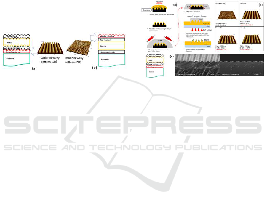
Figure 1: Comparison of the LE structures for TOLEDs in
this work (a) Ordered wavy 1D formed on the bottom-
substrate of TOLED expecting very weak microcavity (b)
Random 2D wavy pattern on the top electrode of TOLED;
maintaining the micro-cavity.
2.1.1 1D Regular Pattern
The pattern of 1D wavy type was fabricated through
thermal reflow process of positive photoresist (PR).
The depth of the pattern was adjusted according to the
spin coating condition of the positive PR. Si wafer-
based master mold with original pattern (height 800
nm, width 800 nm, pitch 1.6 um) was ultrasonically
cleaned using Acetone and IPA and blown with N
2
.
Then dried in an oven at 180°C for 1 hour. Positive
PR (ma-P1205, Microresist corp.) was dropped on the
cleaned master mold and maintained for 2 min, then
spin-coated at 2000 rpm for 60 seconds. When the
spin coating was completed, a wavy pattern was
formed by heating treatment for 10 min on a hot plate
of 100°C. The polydimethylsiloxane (PDMS) was
mixed with the curing agent at a ratio of 10:1 and
poured onto the wavy pattern. It was stored at room
temperature for 24 hours and removed bubbles inside.
The PDMS was thermally cured by storing in an oven
at 60°C for 4 hours. The PDMS replica mold was
separated from the master mold and ultrasonically
cleaned for 10 min in a 1:1 mixture of acetone and
isopropyl alcohol (IPA). Then, using N
2
, it was dried
in an oven at 180°C for 1 hour to produce PDMS
replica mold. The pre-cleaned glass with PR-spin-
coated at 4000 rpm for 60s was pre-baked on a 100°C
hot plate for 1 min. The PDMS replica mold with
wavy pattern was transferred to pre-baked PR by
thermal nanoimprinting lithography (NIL) process.
The thermal NIL process was carried out on a 100
o
C
hot plate and the pressure was applied for 1 hour using
a weight of 1kg or 3kg. Wavy patterns for devices B,
C, and D (atomic force microscopy - AFM image as
seen in Fig. 2b) were prepared by controlling the rpm
of the spin coating process at 2000, 2250, and 2500
rpm.
Figure 2: (a) Schematic fabrication process of a wavy
patterned TOLED by thermal imprinting (b) scale of the 1D
wavy patterns for TOLED device fabrication (c) Cross-
sectional SEM image of wavy pattern produced through
thermal reflow process (magnification: 10k), (left) using 1
kg, (right) 3 kg weight.
2.1.2 2D Irregular/Corrugated Pattern
At least two organic layers (typically for 35nm/15nm-
thick bi-layers) were deposited by thermal
evaporation at a high vacuum system with a base
pressure below 1 x 10
-6
torr without breaking the
vacuum on top of the TOLED devices with
transparent top cathode. After deposition of bi-layer,
the sample was thermal treated at 80
o
C for 10min in
the N
2
chamber for thermal expansion stage. Because
the glass transition temperature of other organic
materials (charge transporting and emission layers) in
TOLEDs were higher than 80
o
C, almost no change of
device without 2D pattern after this thermal
annealing. Followed by the heating, the sample was
cooled to ambient temperature by keeping in the N
2
chamber for 5min. The difference in coefficient of
thermal expansion (CTE) between the bi-layer on top
of transparent electrode of TOLED generated a
spontaneous buckling structure.
2.2 Fabrication of Microcavity OLEDs
Microcavity OLED with top-emission structure were
fabricated by thermal evaporation onto pre-cleaned
glass substrate. All of the following deposition
process were performed through a thermal
Improved Viewing Angle and Light Extraction Efficiency of Microcavity OLED with Corrugated Capping Layer
143
evaporation without breaking vacuum. Aluminum
layer was deposited on glass substrate as a reflective
anode electrode having a thickness of 100 nm.
Afterwards, 2 nm-thick MoO
3
layer for hole injection
and buffer, 28 nm-thick TCTA layer for hole
transport, 30 nm-thick EML layer of doped co-host
system (TCTA : TmPyPB : Ir(ppy)
3
= 0.465 : 0.465 :
0.07), 25 nm-thick TmPyPB layer for electron
transport, 0.5 nm-thick LiF layer and 1 nm-thick Al
layer for electron injection, and 18 nm-thick Ag layer
for composite semi-transparent cathode electrode
were deposited. Surface morphology of sample was
measured by atomic force microscopy (AFM, Veeco
Instruments) and scanning electron microscope
(SEM), etc. Fabricated TOLEDs were characterized
using a source meter (Keithley 2400) with a
spectrometer (PR655, Photo Research) and custom-
built goniometer for angular dependence measure-
ment of light emission. All electroluminescence
spectra and angular emission patterns were recorded
at a constant current density of 10mA/cm
2
with a
spectrometer
2.3 Results of Device Data: Improved
LE and Viewing Angle Behavior
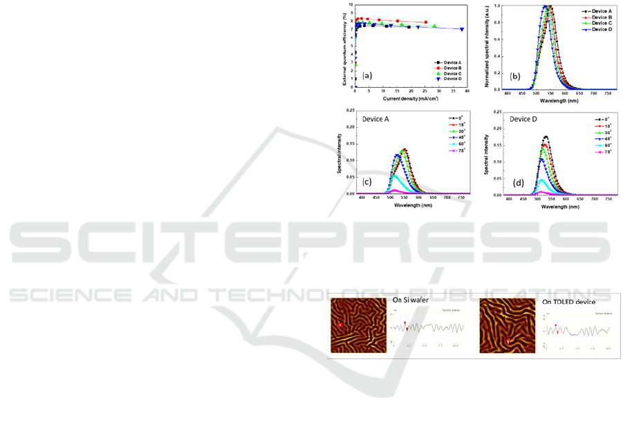
Fig 3 (a) illustrates current density - external quantum
efficiency behavior of TOLED with 1D wavy
underneath of entire layers. The devices with wavy
pattern showed slightly higher current density than
references. At the inflection point of these sinusoidal
patterns, the thickness of the organic layer is partially
thinned, which might result in the formation of a
stronger local electric field. Luminance tended to
increase as the depth of the wavy pattern increases,
however, EQE values are only slightly increased at
device B (low-height 1D wavy) compared to
reference device A, showing only similar values of
7.73 and 7.56% for devices with higher 1D patterns
(device C and D, respectively). Fig 3b shows
normalized spectral intensity in the normal direction
of the emitting surface. The sinusoidal wavy pattern
gradually changes the microcavity length of the
TOLED. The thickness of the cavity length (organic
layer) became thinner at the inflection point and
thickens at the trough peak (Liu et al. 2012). With the
height of wavy patterns inside TOLED increases, the
micro-cavity effect starts to be reduced, so that
angular dependence of the spectrum for device D is
less-sensitive compared with reference device A.
However, overall performance of wave LE layer was
not great for these structures.
Fig 4 illustrate the representative image obtained
by AFM for 2D random wavy patterns that organic
bi-layers with thermal expansivity difference
generates. The pitch and depth of patterns could be
systematically controlled, depending on the annealing
temperature and time. The Si wafer and the buckling
structure formed on the top of the TOLED are shown
in Fig 4a and 4b, respectively. For example, 35nm
N,N’-Bis(3-methylphenyl)-N,N’-diphenylbenzidine
(TPD) and 15nm tris(8-hydroxy-quinolinato)
aluminum (Alq
3
) deposited and annealed at a
temperature of 80°C were shown. The both measured
patterns had 750 nm pitch and 30 nm depth.
Figure 3: (a) Current density v. EQE, (b) spectral response
(c)(d) angular dependence per each viewing angle for
device A and D, without and with 1D micron scale wavy
pattern. Devices are identical with structures in Fig. 2.
Figure 4: AFM image of 2D buckling structure formed by
spontaneous thermal expansion/compression (a) on the Si
wafer substrate and (b) on the TOLED device (scan size: 10
x 10 μm).
Since the formation of buckling 2D wavy patterns
formed on top of the transparent cathode of TOLED
does not affect the thermal state of the underlying
organic layer of devices, micro-cavity of those
TOLEDS were well maintained. Devices in Fig 5a
showed; the layout of LE bucking structures, where
device A (EQE 12.4 represents the reference without
LE, device B shows non-bucking LE with same
organic bi-layer. For devices of C, D, and E, wavy
pattern pitch/depth is 750/30, 1000/45, and 1150/64
(nm), respectively. The improvement of external
quantum efficiencies were significant in case of
TOLEDs with 2D buckling, where the most
optimized devices E showed 21% (reference A and
PHOTOPTICS 2025 - 13th International Conference on Photonics, Optics and Laser Technology
144
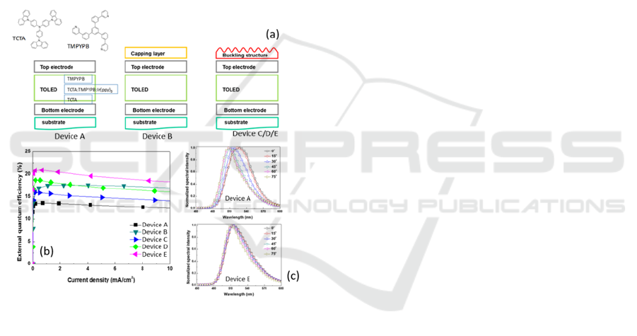
w/o buckling LE device B shows EQE of 13.5 and
17%; see Fig 5b). More than 50% of EQE was
obtained for device with largest 2D wavy LE
structure. Such a result, observed in case of optimum
buckling structure formed on top of the translucent
electrode of device, can be explained by the
suppression of light loss by the SP mode at semi-
transparent metal/air interface without losing the
control of polarization of light. Moreover, the shift of
the maximum peak of electroluminescence for
buckling patterned device was less than 4nm with the
viewing angle range of 0 to 75 degree (>20nm shift
for control device), securing a negligible change of
the spectral characteristics and color stability (robust
viewing angle behavior as for cavity-based device,
comparable results with Kim et al. 2017) as seen in
Fig 5c.
Figure 5: (a) Layout of TOLEDs; reference, flat capping
layer, and 2D buckled layer (same bi-layer) (b) current
density vs. EQE for each TOLEDs with different
flat/buckling LE structures (c) comparison of the angular
dependence for reference device A and 2D buckling device
E.
3 CONCLUSIONS
As for overall evaluation, corrugated “wavy” patterns
at a micron-scale enhances the viewing angle, which
is a significant advantage for display technologies.
Moreover, luminous efficiency was improved by
more than 50% for green phosphorescent TOLEDs as
long as they maintained less-sensitive viewing angle
dependence and stable color purity. It can be noted
that spontaneous formation of 2D wavy buckling
structures through thermal deposition and annealing
is simple and potentially cost-effective.
For 1D corrugated “wavy” patterns at a general
micron-scale, as the aspect ratio of the pattern
becomes larger, the interference phenomenon became
complicated and the viewing angle was improved.
However, efficiency was increased only at limited
condition of low aspect ratio 50:1 to 17:1, where the
larger patterns break the micro-cavity of TOLEDs.
Therefore, this might be a limitation restricting the
practical application of this method for the robustness
of commercial process.
A simple process for the spontaneous formation
of 2D wavy buckling structures generated patterns
with pitches of 750 ~ 1100 nm. These randomly
directed patterns were formed on top of the cathode
(semi-transparent) of TOLEDs by the thermal
deposition and annealing process, which did not
affect the thermal and transition status of the other
organic layers.
Even though the interference phenomenon is
rather complicated, and larger patterns breaking the
micro-cavity of TOLEDs could lead to structural
integrity issues and affect the overall device
performance, the improvement of the luminous
efficiency more than 50 % of the reference shown at
green phosphorescent TOLED will have a strong
impact on the progress of device optimization. Since
this method ensures less-sensitive viewing angle
dependence and stable color purity as well as
efficiency boost-up, this approach can be applied
various kinds of devices having strong micro-cavity
structures, such as TOLEDs with stable color purity
and OLED lasers.
ACKNOWLEDGEMENTS
This study was supported by the Industrial Strategic
Technology Development Program funded by the
Ministry of Trade, Industry and Energy (MOTIE),
South Korea (RS-2024-00417913) and Basic Science
Research Program Through National Research
Foundation of Korea (NRF) funded by the Ministry
of Education, Science and Technology
(2022R1F1A1074725)
REFERENCES
Koo, W. H., Jeong, S. M., Araoka, F., Ishikawa, K.,
Nishimura, S., Toyooka, T, Takezoe, H. (2010), Nat.
Photonics 4, 222
Improved Viewing Angle and Light Extraction Efficiency of Microcavity OLED with Corrugated Capping Layer
145

Koo, W. H., Jeong, S. M., Nishimura, S., Araoka, F.,
Ishikawa, K., Toyooka, T., Takezoe, H. (2011) Adv.
Mater. 23,1003
Yin D., Feng, J., Ma, R., Liu, Y-F., Zhang, Y-L., Zhang, X-
L. Bi, Y-G., Chen, Q-D., Sun, H-B., (2016) Nat. Comm.
7, 11573
Koo, W. H., Chin, B.D., Jo, S. M., (2021) Korea Patent 10-
2293473 “Organic Light Emitting Display Device and
Method of Manufacturing the Same”
Liu, Y. F., Feng, J., Bi, Y. G., Song, J. F., Jin, Y., Bai, Y-
G., Chen, Q-D. Sun, H. B., (2012) Opt. Lett. 37, 124
Kim, E., Chung, J., Lee, J., Cho, H., Cho, N. S., Yoo, S.,
(2017) Organic Electronics 48, 348
PHOTOPTICS 2025 - 13th International Conference on Photonics, Optics and Laser Technology
146
